
Texas Instruments
SN74LVC1G10DSFR

Why Choose Us?
Professional Platform
B2B & B2C purchasingDelivery at full speed
1-2 days deliveryWide variety
Original manufacturers365 days guarantee
Responsible quality
.png)


Tech Specifications
SN74LVC1G10DSFR Description
The Texas Instruments SN74LVC1G10DSFR is a single gate buffer and line driver with a 3-state output. Here's a brief description of the model, its features, and potential applications:
Model Description:
The SN74LVC1G10DSFR is a member of the 74LVC1G10 series, which is a family of low voltage logic gates designed for high-speed applications. This particular model functions as a buffer and line driver, which means it can receive an input signal and provide a buffered output signal that is identical to the input, with the added ability to drive longer lines or multiple loads.
Features:
- 3-State Output: The device has a 3-state output, which means it can actively drive the output high, low, or be in a high-impedance state (off).
- Low Voltage Operation: It operates at low voltages, making it suitable for modern low-power systems.
- High-Speed Performance: Designed for high-speed applications, it can quickly switch between states.
- Low Power Consumption: Despite its high-speed capabilities, the SN74LVC1G10DSFR is designed to consume low power, which is beneficial for battery-powered or energy-sensitive applications.
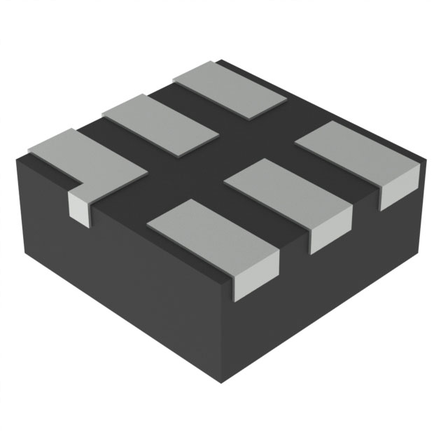
- Small Package Size: It comes in a small DFN (Dual Flat No-leads) package, which is ideal for space-constrained applications.
Applications:
- Line Drivers: In systems where signals need to be transmitted over longer distances without significant degradation, the SN74LVC1G10DSFR can be used as a line driver to boost the signal strength.
- Buffers: It can be used to buffer signals to ensure that the output is not affected by the input's loading characteristics.
- Bus Transceivers: In computer systems and other digital electronics, it can be used as a bus transceiver to interface with different voltage levels.
- Automotive Applications: Due to its robustness and low power consumption, it can be used in automotive electronics for signal conditioning and buffering.
- Industrial Control Systems: In industrial settings where reliability and speed are crucial, this device can be used to ensure signal integrity across various components.
It's important to note that the specific applications would depend on the system requirements and design considerations. The SN74LVC1G10DSFR is just one component that can be used in a broader design context to achieve the desired functionality.
FAQ
| Quantity | Unit Price | Ext. Price |
|---|---|---|
| 5+ | $0.21643 | $1.08 |
| 50+ | $0.17040 | $8.52 |
| 150+ | $0.15065 | $22.60 |
Not available to buy online? Want the lower wholesale price? Please Send RFQ to get best price, we will respond immediately


.png?x-oss-process=image/format,webp/resize,h_32)


