
 German
 Japanese
 Portuguese
 Korea
Korea
 Mexico
 Dutch
Dutch


Texas Instruments
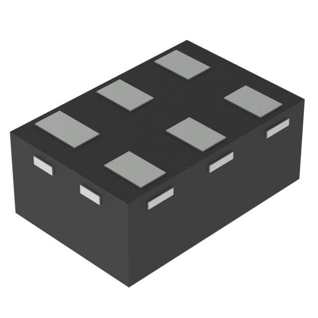
SN74LVC1G125DRYR

Why Choose Us?
Professional Platform
B2B & B2C purchasingDelivery at full speed
1-2 days deliveryWide variety
Original manufacturers365 days guarantee
Responsible quality
.png)


Tech Specifications
SN74LVC1G125DRYR Description
The SN74LVC1G125DRYR is a single gate from Texas Instruments' 74LVC1G125 series. It is a non-inverting buffer and line driver with a 1.65V to 3.6V operating voltage range. The device is available in a small DFN (Dual Flat No-Leads) package, making it suitable for space-constrained applications.
Description:
The SN74LVC1G125DRYR is a high-speed Si-gate CMOS device that provides excellent performance in a wide range of applications. It is designed to handle high-frequency signals and offers low power consumption, making it ideal for portable and battery-powered devices.
Features:
- Non-inverting buffer and line driver functionality
- 1.65V to 3.6V operating voltage range
- High-speed operation with a propagation delay of 3.5 ns (typical)
- Low power consumption: 1.6 mA (typical) at 3.3V supply voltage
- Wide operating temperature range: -40°C to 125°C
- Available in a small DFN package (1mm x 1mm)
- ESD protection: HBM (Human Body Model) up to 2000V
Applications:
- General-purpose buffering and signal conditioning
- High-speed data transmission and communication interfaces
- Digital signal processing systems
- Battery-powered and portable devices
- Industrial control and automation systems
- Consumer electronics, such as smartphones, tablets, and wearable devices
- Automotive applications, including infotainment systems and control modules
The SN74LVC1G125DRYR is a versatile and reliable device that can be used in a wide range of applications where high-speed signal transmission and low power consumption are essential. Its small form factor and wide operating voltage range make it suitable for both space-constrained and power-sensitive applications.
FAQ
| Quantity | Unit Price | Ext. Price |
|---|---|---|
| 1+ | $0.22000 | $0.22 |
| 10+ | $0.14872 | $1.49 |
| 25+ | $0.13200 | $3.30 |
| 100+ | $0.11290 | $11.29 |
| 250+ | $0.10388 | $25.97 |
Not available to buy online? Want the lower wholesale price? Please Send RFQ to get best price, we will respond immediately


.png?x-oss-process=image/format,webp/resize,h_32)


