
Texas Instruments
SN74LVC1G14DBVTE4
Gates and Inverters


.png?x-oss-process=image/format,webp/resize,p_30)


SN74LVC1G14DBVTE4 Description
SN74LVC1G14DBVTE4 Description
The SN74LVC1G14DBVTE4 is a single-channel inverter IC designed for high-performance digital logic applications. Manufactured by Texas Instruments, this device is part of the 74LVC series, known for its robustness and versatility. The SN74LVC1G14DBVTE4 features a Schmitt trigger input, which provides excellent noise immunity and ensures stable operation in noisy environments. It operates within a wide supply voltage range of 1.65V to 5.5V, making it suitable for various power supply configurations.
The device has a maximum propagation delay of 6.5ns at 2.5V with a load capacitance of 50pF, ensuring fast signal processing and minimal latency. This inverter is designed with a single input and a single circuit, making it ideal for compact designs where space is a constraint. The input logic levels are specified as 0.39V to 1.87V for low and 1.16V to 3.33V for high, providing compatibility with a wide range of digital systems.
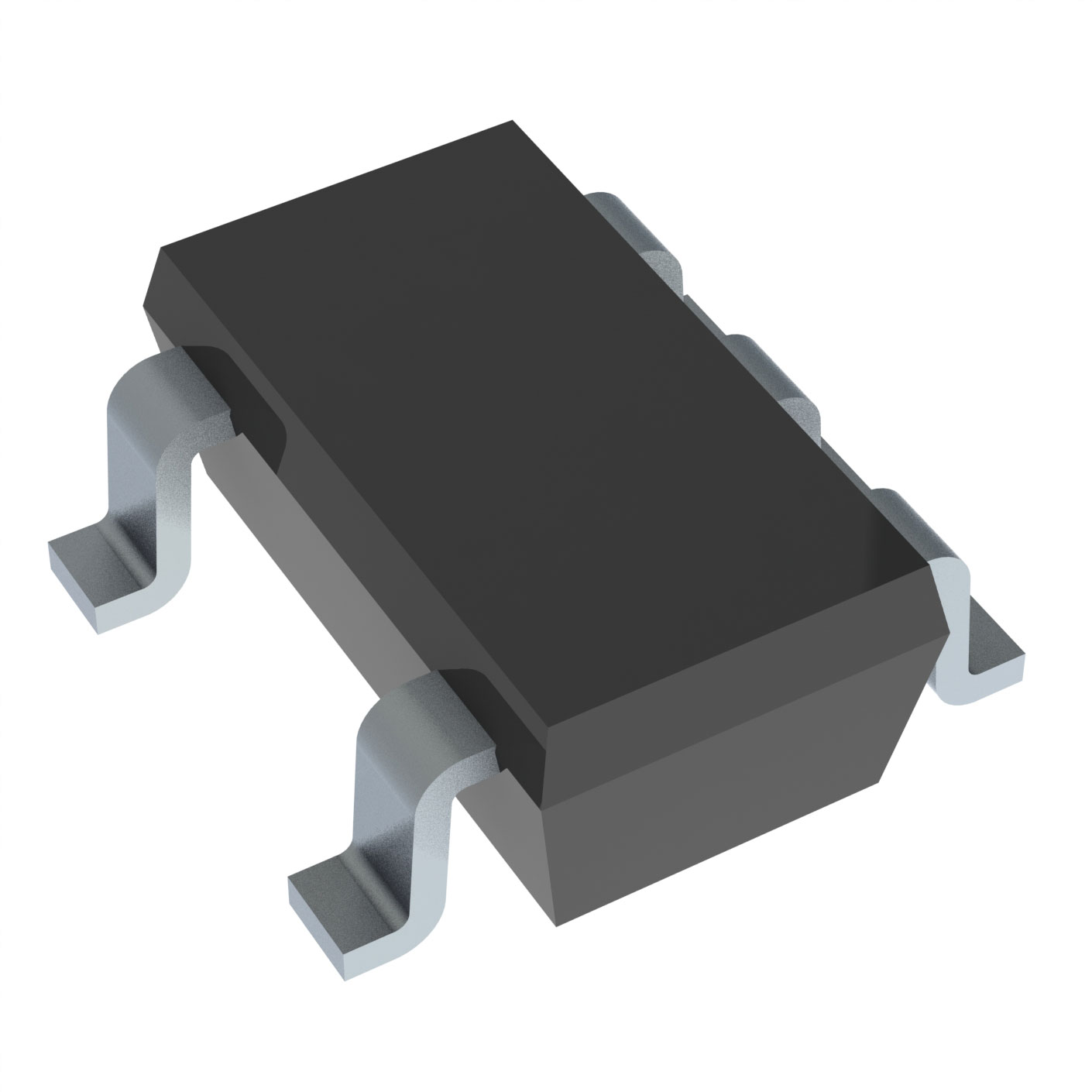
The SN74LVC1G14DBVTE4 is packaged in a Surface Mount SOT23-5 package, which is ideal for automated assembly processes and contributes to the overall compactness of the design. The device is RoHS3 compliant and REACH unaffected, ensuring compliance with environmental regulations and standards.
SN74LVC1G14DBVTE4 Features
- Schmitt Trigger Input: Enhances noise immunity, ensuring stable operation in noisy environments.
- Wide Operating Voltage Range: 1.65V to 5.5V, providing flexibility for various power supply configurations.
- Fast Propagation Delay: 6.5ns at 2.5V with 50pF load capacitance, ensuring high-speed signal processing.
- Low Quiescent Current: Maximum of 10 µA, contributing to energy efficiency.
- High Output Current Capability: 32mA for both high and low outputs, supporting robust signal driving.
- Surface Mount Packaging: SOT23-5 package, suitable for automated assembly and compact designs.
- Environmental Compliance: RoHS3 compliant and REACH unaffected, meeting industry standards for environmental sustainability.
SN74LVC1G14DBVTE4 Applications
The SN74LVC1G14DBVTE4 is ideal for a variety of applications where high-speed signal inversion and noise immunity are critical. Some specific use cases include:
- Digital Signal Processing: Inverting digital signals in high-speed communication systems.
- Noise-Prone Environments: Applications where signals are susceptible to noise, such as industrial control systems.
- Compact Designs: Suitable for space-constrained designs due to its small SOT23-5 package.
- Power-Efficient Systems: Ideal for battery-operated devices or systems where low power consumption is essential.
- Automotive Electronics: Robustness and compliance with environmental standards make it suitable for automotive applications.
Conclusion of SN74LVC1G14DBVTE4
The SN74LVC1G14DBVTE4 is a versatile and high-performance inverter IC that offers significant advantages over similar models. Its wide operating voltage range, fast propagation delay, and Schmitt trigger input make it ideal for a variety of applications, particularly those requiring high-speed signal processing and noise immunity. The compact SOT23-5 package and low quiescent current further enhance its suitability for space-constrained and power-efficient designs. With its environmental compliance and robust performance, the SN74LVC1G14DBVTE4 is a reliable choice for modern digital logic applications.
Tech Specifications
SN74LVC1G14DBVTE4 Documents
Download datasheets and manufacturer documentation for SN74LVC1G14DBVTE4
 Additional Assembly sites 21/Sep/2021
  SN74LVC1G14
 Shopping Guide


.png?x-oss-process=image/format,webp/resize,h_32)


