
Texas Instruments
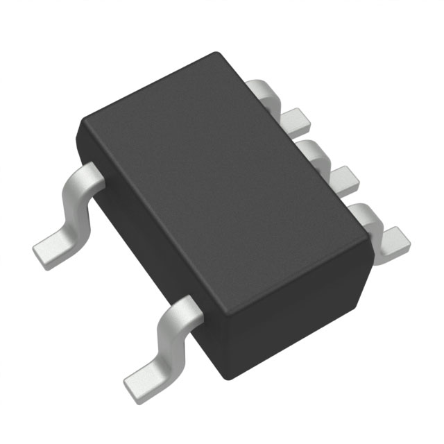
SN74LVC1G17DCK3
Buffers, Drivers, Receivers, Transceivers


- 5+
- $0.09545
- $0.48
- 50+
- $0.07704
- $3.85
- 150+
- $0.06758
- $10.14

.png?x-oss-process=image/format,webp/resize,p_30)


SN74LVC1G17DCK3 Description
SN74LVC1G17DCK3 Description
The SN74LVC1G17DCK3 is a high-performance buffer from Texas Instruments, designed to provide reliable signal conditioning in various electronic systems. This single-bit buffer features a Schmitt Trigger input, which helps to eliminate noise and ensure accurate signal transmission. With a wide supply voltage range of 1.65V to 5.5V, the SN74LVC1G17DCK3 is suitable for a variety of low-voltage applications.
SN74LVC1G17DCK3 Features
- Schmitt Trigger Input: Provides noise immunity and ensures clean signal transmission.
- 1.65V to 5.5V Supply Voltage Range: Suitable for low-voltage applications.
- 1-bit Buffer: Ideal for single-bit signal conditioning.
- Surface Mount: Facilitates integration into compact electronic designs.
- ROHS3 Compliant: Meets environmental regulations for lead-free manufacturing.
- REACH Unaffected: Compliant with the European Union's Registration, Evaluation, Authorization, and Restriction of Chemicals (REACH) regulations.
- 32mA Output Current: Capable of driving heavy loads.
- Moisture Sensitivity Level 1: Suitable for use in a wide range of environmental conditions.
SN74LVC1G17DCK3 Applications
The SN74LVC1G17DCK3 is ideal for use in various applications where signal conditioning and buffering are required. Some specific use cases include:
- Digital Signal Processing: Buffering and conditioning signals in digital signal processing systems.
- Communication Systems: Ensuring clean signal transmission in communication systems, such as wireless and wired networks.
- Automotive Electronics: Buffering signals in automotive control systems and infotainment systems.
- Industrial Control Systems: Providing reliable signal conditioning in industrial control systems and automation equipment.
Conclusion of SN74LVC1G17DCK3
The SN74LVC1G17DCK3 is a versatile and reliable buffer from Texas Instruments, offering a wide supply voltage range, Schmitt Trigger input, and high output current capabilities. Its unique features, such as ROHS3 compliance and REACH unaffected status, make it an excellent choice for a variety of electronic systems. With its ability to handle heavy loads and provide noise immunity, the SN74LVC1G17DCK3 is an ideal solution for applications requiring robust signal conditioning and buffering.
Tech Specifications
SN74LVC1G17DCK3 Documents
Download datasheets and manufacturer documentation for SN74LVC1G17DCK3
 SN74LVC1G17
 Shopping Guide


.png?x-oss-process=image/format,webp/resize,h_32)


