
Texas Instruments
SN74LVC1G17DCKR
Buffers, Drivers, Receivers, Transceivers


.png?x-oss-process=image/format,webp/resize,p_30)


SN74LVC1G17DCKR Description
SN74LVC1G17DCKR Description
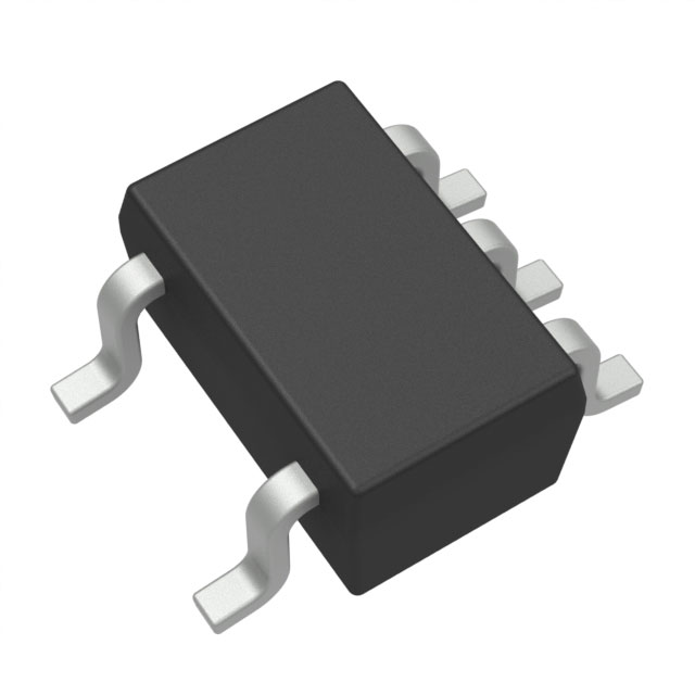
The SN74LVC1G17DCKR from Texas Instruments is a single Schmitt-trigger buffer gate designed for high-performance logic applications. Packaged in a compact SC70-5 form factor, this device operates over a wide voltage range of 1.65V to 5.5V, making it versatile for mixed-voltage systems. As part of the 74LVC series, it combines low power consumption with robust 32mA output drive (both sourcing and sinking), ensuring reliable signal conditioning in noise-sensitive environments. Its Schmitt-trigger input provides hysteresis, improving noise immunity and signal integrity, which is critical for slow or noisy input transitions. The device is RoHS3 compliant and rated for MSL 1 (Unlimited), ensuring suitability for automated assembly processes.
SN74LVC1G17DCKR Features
- Schmitt-Trigger Input: Enhances noise rejection and ensures clean output transitions even with degraded input signals.
- Wide Voltage Range (1.65V–5.5V): Compatible with 1.8V, 2.5V, 3.3V, and 5V logic levels, ideal for mixed-voltage designs.
- High Output Drive (32mA): Capable of driving capacitive loads or multiple inputs without additional buffering.
- Low Power Consumption: Optimized for battery-powered and portable applications.
- Space-Efficient SC70-5 Package: Minimizes board footprint, suitable for high-density layouts.
- Robust ESD Protection: Exceeds industry standards for electrostatic discharge tolerance.
- Industrial-Grade Reliability: Operates across extended temperature ranges with stable performance.
SN74LVC1G17DCKR Applications
- Signal Conditioning: Cleans up noisy or slow-rising signals in sensor interfaces, debouncing switches, or clock distribution networks.
- Voltage Level Translation: Bridges logic levels between disparate voltage domains (e.g., 1.8V to 3.3V).
- Portable Electronics: Ideal for smartphones, wearables, and IoT devices due to low power and small size.
- Industrial Control Systems: Provides noise immunity in PLCs, motor controllers, and automation equipment.
- Consumer Electronics: Used in remote controls, gaming peripherals, and audio/video interfaces for signal integrity.
Conclusion of SN74LVC1G17DCKR
The SN74LVC1G17DCKR stands out as a high-reliability, space-efficient buffer with Schmitt-trigger inputs, addressing critical challenges in modern electronics. Its combination of wide voltage range, high noise immunity, and strong output drive makes it superior to standard buffers in demanding environments. Whether for level shifting, signal cleanup, or power-sensitive designs, this device delivers consistent performance while minimizing board space and power consumption. Engineers can leverage its robustness in applications ranging from consumer gadgets to industrial systems, ensuring design flexibility and long-term reliability.
Tech Specifications
SN74LVC1G17DCKR Documents
Download datasheets and manufacturer documentation for SN74LVC1G17DCKR
 Mult Devices 02/Oct/2017
  SN74LVC1G17
  Copper Bond Wire 07/May/2014 Copper Wire Revision A 03/Nov/2014
 Shopping Guide


.png?x-oss-process=image/format,webp/resize,h_32)


