

Texas Instruments
SN74LVC1G17DRLRG4
Buffers, Drivers, Receivers, Transceivers

Not available to buy online? Want the lower wholesale price? Please Send RFQ to get best price, we will respond immediately


.png?x-oss-process=image/format,webp/resize,p_30)


SN74LVC1G17DRLRG4 Description
SN74LVC1G17DRLRG4 Description
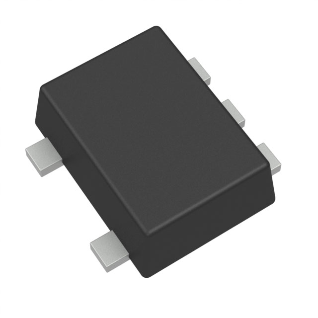
The SN74LVC1G17DRLRG4 from Texas Instruments is a single Schmitt-trigger buffer designed for 1.65V to 5.5V voltage operation, making it compatible with a wide range of logic levels. Housed in a compact SOT-5 package, this device is optimized for space-constrained applications while delivering robust performance. As part of the 74LVC series, it features Schmitt-trigger inputs for improved noise immunity and signal integrity, ensuring reliable operation in noisy environments. With 32mA output drive capability, it supports both high and low current demands, making it suitable for interfacing with various loads.
SN74LVC1G17DRLRG4 Features
- Schmitt-Trigger Inputs: Enhances noise rejection and ensures clean signal transitions.
- Wide Voltage Range (1.65V–5.5V): Compatible with mixed-voltage systems, including 3.3V and 5V logic.
- High Output Drive (32mA): Capable of driving moderate loads directly.
- Single-Channel Design: Ideal for applications requiring minimal footprint and power.
- RoHS3 Compliant & REACH Unaffected: Meets environmental and regulatory standards.
- Surface-Mount (SOT-5) Packaging: Optimized for automated assembly and PCB space efficiency.
- Unlimited MSL Rating (Level 1): No moisture sensitivity concerns during storage or handling.
SN74LVC1G17DRLRG4 Applications
This buffer is particularly suited for:
- Signal Conditioning: Cleans up noisy or slow-rising signals in sensor interfaces.
- Level Shifting: Bridges voltage gaps between 1.8V, 3.3V, and 5V systems.
- Clock Buffering: Ensures stable clock distribution in low-power embedded systems.
- Portable Electronics: Ideal for smartphones, wearables, and IoT devices due to its small size and low-voltage operation.
- Industrial Control Systems: Provides reliable signal buffering in harsh environments.
Conclusion of SN74LVC1G17DRLRG4
The SN74LVC1G17DRLRG4 stands out for its Schmitt-trigger robustness, wide voltage flexibility, and compact form factor, making it a versatile choice for modern electronics. Its high noise immunity and strong output drive make it superior to standard buffers in challenging conditions. Whether for consumer, industrial, or automotive applications, this device ensures reliable signal integrity while minimizing board space and power consumption.
Tech Specifications
SN74LVC1G17DRLRG4 Documents
Download datasheets and manufacturer documentation for SN74LVC1G17DRLRG4
SN74LVC1G17 Related Parts


Shopping Guide


.png?x-oss-process=image/format,webp/resize,h_32)


©2025 ERSA Electronics Corporation.