
Texas Instruments
SN74LVC1G34DBVTE4
Buffers, Drivers, Receivers, Transceivers


.png?x-oss-process=image/format,webp/resize,p_30)


SN74LVC1G34DBVTE4 Description
SN74LVC1G34DBVTE4 Description
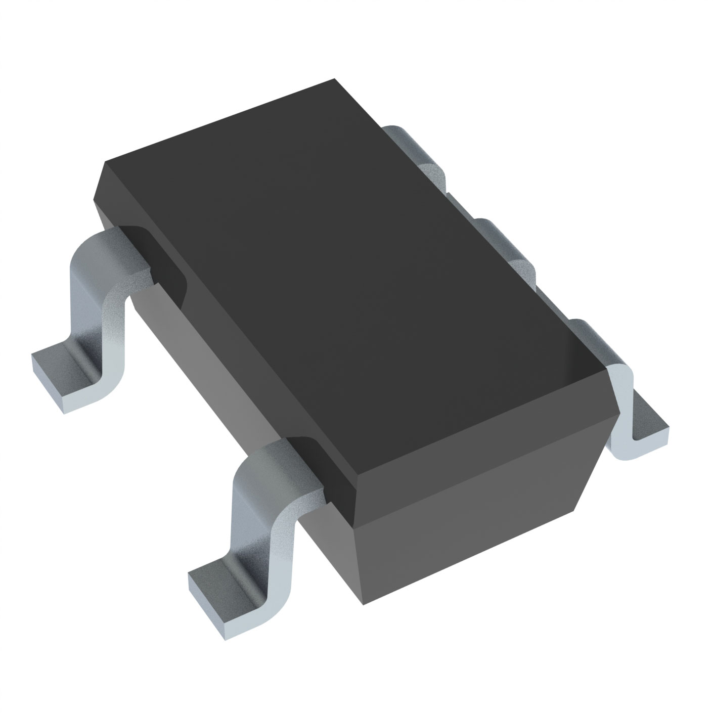
The SN74LVC1G34DBVTE4 is a single non-inverting buffer designed by Texas Instruments, a leading manufacturer in the semiconductor industry. This device is part of the 74LVC series, known for its high performance and reliability. The SN74LVC1G34DBVTE4 features a single bit per element and is optimized for surface mount applications, making it ideal for compact and high-density designs. It operates within a wide voltage range of 1.65V to 5.5V, ensuring compatibility with various power supply configurations. The device is packaged in a SOT23-5 package, which is both space-efficient and robust for surface mount technology (SMT) processes.
SN74LVC1G34DBVTE4 Features
- Wide Operating Voltage Range: The SN74LVC1G34DBVTE4 operates within a voltage range of 1.65V to 5.5V, providing flexibility in power supply options and ensuring compatibility with a variety of systems.
- High Current Capability: This buffer offers a high current output capability of 32mA for both high and low states, making it suitable for driving multiple loads or interfacing with various types of devices.
- Non-Inverting Buffer: The non-inverting functionality ensures that the output signal maintains the same logic state as the input, simplifying circuit design and reducing complexity.
- Surface Mount Technology: The SOT23-5 package is designed for surface mount applications, enabling high-density PCB layouts and efficient manufacturing processes.
- Compliance and Safety: The device is REACH unaffected and RoHS3 compliant, ensuring it meets the latest environmental and safety standards. It also has a moisture sensitivity level (MSL) of 1, making it suitable for unlimited exposure to standard manufacturing environments.
- Packaging: The SN74LVC1G34DBVTE4 is available in tape and reel (TR) packaging, facilitating automated assembly and ensuring consistent quality.
SN74LVC1G34DBVTE4 Applications
The SN74LVC1G34DBVTE4 is well-suited for a variety of applications where signal buffering and voltage level translation are required. Some specific use cases include:
- Digital Signal Processing: In systems where digital signals need to be buffered or level-shifted, the SN74LVC1G34DBVTE4 provides a reliable and efficient solution.
- Microcontroller Interfaces: The device can be used to interface microcontrollers with various peripherals, ensuring signal integrity and compatibility.
- Communication Systems: In communication circuits, the buffer can drive signals over longer distances or through multiple loads without significant degradation.
- Consumer Electronics: The compact size and high performance make it ideal for consumer electronics where space is limited and reliability is crucial.
- Industrial Control Systems: The robustness and wide operating voltage range make it suitable for industrial applications where environmental conditions can be harsh.
Conclusion of SN74LVC1G34DBVTE4
The SN74LVC1G34DBVTE4 is a versatile and high-performance single non-inverting buffer that offers significant advantages over similar models. Its wide operating voltage range, high current output capability, and compact SOT23-5 package make it an excellent choice for a variety of applications. The device's compliance with environmental and safety standards ensures it meets the requirements of modern electronics manufacturing. Whether used in digital signal processing, microcontroller interfaces, or industrial control systems, the SN74LVC1G34DBVTE4 provides reliable performance and ease of integration.
Tech Specifications
SN74LVC1G34DBVTE4 Documents
Download datasheets and manufacturer documentation for SN74LVC1G34DBVTE4
 Mechanical Outline Drawing
  Product Change Notification (PDF)
  SN74LVC1G34DBVTE4 Symbol & Footprint by SnapMagic
  Logic Guide (Rev. AB) Little Logic Guide 2018 (Rev. G)
  Drive Transmission Lines With Logic Redrive Digital Signals
  SN74LVC1G34 Behavioral SPICE Model
 Shopping Guide


.png?x-oss-process=image/format,webp/resize,h_32)


