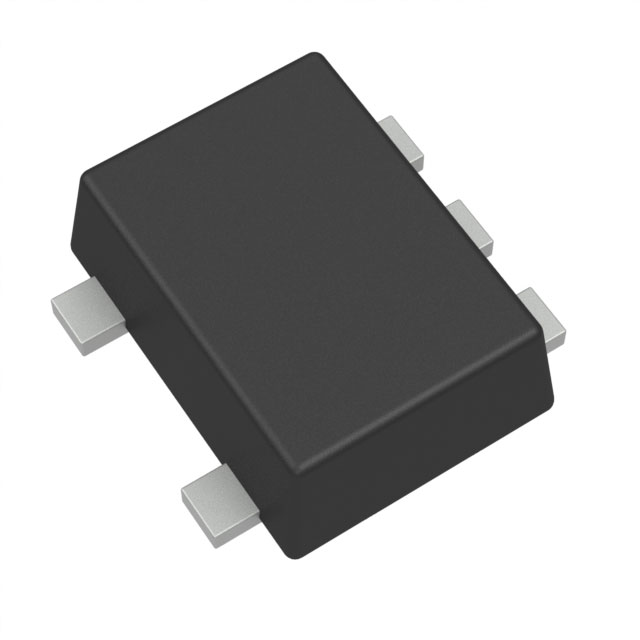
Texas Instruments_SN74LVC1G66DRLR

Texas Instruments
SN74LVC1G66DRLR  
Analog Switches, Multiplexers, Demultiplexers

Texas Instruments
SN74LVC1G66DRLR
747-SN74LVC1G66DRLR
Ersa
Texas Instruments-SN74LVC1G66DRLR-datasheets-1101309.pdf
IC SWITCH SPST-NO X 1 10OHM SOT5
In Stock : 20278

Not available to buy online? Want the lower wholesale price? Please Send RFQ to get best price, we will respond immediately

QUICK RFQ
ADD TO RFQ LIST
ersa FreeSample ersa flow
  • Quantity
  • Unit Price
  • Ext. Price
    • 5+
    • $0.07113
    • $0.36
    • 50+
    • $0.06957
    • $3.48
    • 150+
    • $0.06851
    • $10.28
    ADD TO CART
    QUICK ORDER
    $0.00000    $0.00
    ISO9001
    Quality Policy
    ISO45001
    ISO14001

    SN74LVC1G66DRLR Description

    The SN74LVC1G66DRLR is a single gate buffer and line driver from Texas Instruments. It is a part of the 74LVC1Gxx family of logic devices that are designed to provide low voltage and low power operation while maintaining high performance.

    Description:

    The SN74LVC1G66DRLR is a single gate buffer and line driver that provides high-speed signal buffering and line driving capabilities. It is available in a small SOT-23 package, making it ideal for use in compact and portable applications.

    Features:

    1. Low voltage operation: The SN74LVC1G66DRLR operates from a supply voltage range of 1.65V to 3.6V, making it suitable for use in low-voltage systems.
    2. Low power consumption: The device has a low power consumption of just 1.2mA, which makes it ideal for battery-powered applications.
    3. High-speed performance: The SN74LVC1G66DRLR has a propagation delay of just 3.5ns, making it suitable for high-speed applications.
    4. Wide operating temperature range: The device can operate over a wide temperature range of -40°C to +125°C, making it suitable for use in harsh environments.
    5. ESD protection: The SN74LVC1G66DRLR has built-in electrostatic discharge (ESD) protection, which helps to protect the device from damage due to static electricity.

    Applications:

    The SN74LVC1G66DRLR is suitable for a wide range of applications, including:

    1. Signal buffering in low-voltage systems
    2. Line driving in high-speed communication systems
    3. Level shifting between different voltage domains
    4. Glitch-free switching in digital systems
    5. Battery-powered applications where low power consumption is critical
    6. Industrial control systems where high reliability and wide operating temperature range are required.

    Overall, the SN74LVC1G66DRLR is a versatile and high-performance single gate buffer and line driver that offers low voltage and low power operation, making it suitable for a wide range of applications.

    Tech Specifications

    Number of Channels per Chip
    Power Supply Type
    Output Signal Type
    Configuration
    Crosstalk
    PPAP
    Maximum Turn-On Time (ns)
    Product Status
    Voltage - Supply, Dual (V±)
    Automotive
    Supplier Package
    Channel Capacitance (CS(off), CD(off))
    Package / Case
    On-State Resistance (Max)
    REACH Status
    Multiplexer/Demultiplexer Circuit
    EU RoHS
    Switch Time (Ton, Toff) (Max)
    Maximum Turn-Off Time (ns)
    Moisture Sensitivity Level (MSL)
    Operating Temperature
    Maximum Frequency (25°C) @ Vcc (MHz)
    ECCN
    Mounting Type
    Standard Package Name
    Maximum On Resistance Range (Ohm)
    Pin Count
    Mounting
    Input Signal Type
    Minimum Single Supply Voltage (V)
    Lead Shape
    HTSUS
    Package
    Switch Architecture
    Current - Leakage (IS(off)) (Max)
    PCB changed
    HTS
    ECCN (US)
    Supplier Device Package
    Minimum Operating Temperature (°C)
    Maximum Operating Temperature (°C)
    Channel-to-Channel Matching (ΔRon)
    Propagation Delay Test Condition (pF)
    Package Height
    Mfr
    Polarity
    Charge Injection
    Maximum On Resistance (Ohm)
    RoHS Status
    Typical Single Supply Voltage (V)
    Number of Inputs per Chip
    Maximum Propagation Delay Bus to Bus (ns)
    -3db Bandwidth
    Number of Outputs per Chip
    Chip Enable Signals
    Package Length
    Maximum Supply Current (mA)
    Voltage - Supply, Single (V+)
    Series
    Type
    Maximum Single Supply Voltage (V)
    Switch Circuit
    Part Status
    Number of Circuits
    Package Width
    Base Product Number
    On Time - Max
    Maximum Dual Supply Voltage
    Unit Weight
    Off Time - Max
    Minimum Dual Supply Voltage
    Supply Current - Max
    RoHS
    Supply Voltage - Min
    Number of Channels
    Height
    Maximum Operating Temperature
    Supply Voltage - Max
    Width
    Switch Continuous Current
    Mounting Style
    On Resistance - Max
    Minimum Operating Temperature
    Length
    Supply Type
    USHTS

    SN74LVC1G66DRLR Documents

    Download datasheets and manufacturer documentation for SN74LVC1G66DRLR

    Ersa Mechanical Outline Drawing      
    Ersa Product Change Notification_2024_12_19 (PDF)       Product Change Notification (PDF)      
    Ersa SN74LVC1G66DRLR Symbol & Footprint by SnapMagic      
    Ersa Logic Guide (Rev. AB)       Little Logic Guide 2018 (Rev. G)      
    Ersa HSPICE MODEL OF SN74LVC1G66      

    Shopping Guide

    Payment Methods
    Payment Methods include Prepayment TT (bank transfer), Western Union, and PayPal. Customers are responsible for shipping costs, bank charges, customs duties and taxes.
    Shipping Rate
    Shipments are made once a day around 5pm, excluding Sundays. Once shipped, the estimated delivery time is usually 5-7 business days, depending on the courier you choose.
    Delivery Methods
    Provide DHL, FedEx, UPS, EMS, SF Express and Registered Airmail International Delivery Service