
Texas Instruments
SN74LVC1G98DRLR
Multi-Function, Configurable Gates and Inverters


.png?x-oss-process=image/format,webp/resize,p_30)


SN74LVC1G98DRLR Description
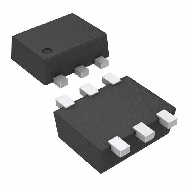
The Texas Instruments SN74LVC1G98DRLR is a high-speed 2-input quaternary (4-input) AND gate in a 1.65mm ultra low profile QFN package. It belongs to the 74LVC1Gxx family of single gate logic devices, which are designed for low voltage and low power applications.
Description:
The SN74LVC1G98DRLR is a single gate logic device that performs a logical AND operation on two input signals. It has two inputs (A and B) and one output (Y). When both inputs are high (logic 1), the output is also high (logic 1). If either input is low (logic 0), the output is low (logic 0).
Features:
- High-speed performance: The SN74LVC1G98DRLR has a fast propagation delay of 3.5 ns (typical), making it suitable for high-speed applications.
- Low voltage operation: It operates with a supply voltage range of 1.65V to 3.6V, making it compatible with modern low voltage systems.
- Low power consumption: The device has a low power consumption of 1.4 mW (typical), which is suitable for battery-powered or energy-efficient applications.
- 1.65mm ultra low profile QFN package: The compact package size of 1.65mm x 2mm makes it suitable for space-constrained applications.
- Wide operating temperature range: The SN74LVC1G98DRLR can operate in a temperature range of -40°C to +125°C, making it suitable for various industrial and automotive applications.
- ESD protection: The device features built-in electrostatic discharge (ESD) protection, ensuring robust performance in noisy environments.
Applications:
- Digital logic circuits: The SN74LVC1G98DRLR can be used in digital logic circuits for signal processing, data manipulation, and control applications.
- Microcontroller input/output expansion: It can be used to expand the input/output capabilities of microcontrollers in embedded systems.
- Communication systems: The high-speed performance of the device makes it suitable for use in communication systems, such as serial interfaces and data buses.
- Automotive applications: The wide operating temperature range and ESD protection make the SN74LVC1G98DRLR suitable for use in automotive electronics, such as control modules and sensor interfaces.
- Industrial control systems: The device can be used in various industrial control systems, such as programmable logic controllers (PLCs) and motor control circuits.
- Battery-powered devices: The low power consumption of the SN74LVC1G98DRLR makes it suitable for use in battery-powered devices, such as portable electronics and wireless communication devices.
In summary, the Texas Instruments SN74LVC1G98DRLR is a high-speed, low-voltage, and low-power 2-input AND gate that offers a compact package size and wide operating temperature range. It is suitable for various applications, including digital logic circuits, microcontroller input/output expansion, communication systems, automotive applications, industrial control systems, and battery-powered devices.
Tech Specifications
SN74LVC1G98DRLR Documents
Download datasheets and manufacturer documentation for SN74LVC1G98DRLR
 Mult Dev Assembly 14/Dec/2023
  SN74LVC1G98
  SN74LVC1G98
 Shopping Guide


.png?x-oss-process=image/format,webp/resize,h_32)


