

Texas Instruments
SN74LVC244ADWG4
Buffers, Drivers, Receivers, Transceivers

Not available to buy online? Want the lower wholesale price? Please Send RFQ to get best price, we will respond immediately


.png?x-oss-process=image/format,webp/resize,p_30)


SN74LVC244ADWG4 Description
SN74LVC244ADWG4 Description
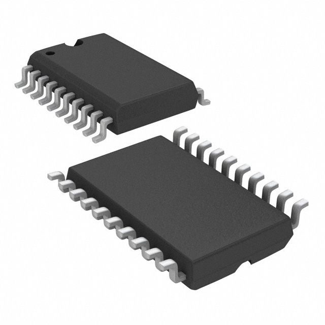
The SN74LVC244ADWG4 is a high-performance, non-inverting buffer IC designed by Texas Instruments, a leading manufacturer in the semiconductor industry. This Logic IC Chip is part of the 74LVC series, known for its robust performance and reliability. The SN74LVC244ADWG4 features a 20SOIC package, making it suitable for surface mount applications. It operates within a wide voltage range of 1.65V to 3.6V, providing flexibility in various electronic designs.
This IC is composed of two 4-bit non-inverting buffers, offering a total of 8 buffered outputs. Each buffer can handle a maximum output current of 24mA, both for high and low states, ensuring robust signal transmission. The SN74LVC244ADWG4 is REACH unaffected and ROHS3 compliant, adhering to stringent environmental and safety standards. It is also classified under HTSUS code 8542.39.0001 and has a moisture sensitivity level (MSL) of 1, making it suitable for unlimited storage conditions.
SN74LVC244ADWG4 Features
- Wide Operating Voltage Range: The SN74LVC244ADWG4 operates within a voltage range of 1.65V to 3.6V, making it versatile for different power supply configurations.
- High Output Current Capability: Each output pin can source or sink up to 24mA, ensuring strong signal drive capabilities.
- Non-Inverting Buffers: The IC includes two 4-bit non-inverting buffers, providing a total of 8 buffered outputs, ideal for signal amplification and conditioning.
- Surface Mount Compatibility: The 20SOIC package is designed for surface mount technology, enabling compact and efficient PCB designs.
- Environmental Compliance: The SN74LVC244ADWG4 is REACH unaffected and ROHS3 compliant, ensuring it meets environmental and safety standards.
- Moisture Sensitivity Level: With an MSL of 1, the IC can be stored indefinitely without the need for special handling or packaging.
SN74LVC244ADWG4 Applications
The SN74LVC244ADWG4 is ideal for a variety of applications where signal buffering and amplification are required. Its wide operating voltage range and high output current make it suitable for:
- Digital Signal Processing: Amplifying and conditioning digital signals in microcontroller and microprocessor-based systems.
- Interface Circuits: Enhancing signal integrity in communication interfaces, such as SPI and I2C.
- Memory Systems: Buffering address and data lines in memory modules.
- Consumer Electronics: Improving signal quality in devices such as smartphones, tablets, and gaming consoles.
- Industrial Automation: Ensuring reliable signal transmission in control systems and sensors.
Conclusion of SN74LVC244ADWG4
The SN74LVC244ADWG4 from Texas Instruments is a versatile and reliable non-inverting buffer IC. Its wide operating voltage range, high output current capability, and compact surface mount package make it an excellent choice for a variety of electronic applications. The IC's compliance with environmental and safety standards ensures it meets the demands of modern electronics manufacturing. Whether used in digital signal processing, interface circuits, or consumer electronics, the SN74LVC244ADWG4 provides robust performance and reliability, making it a standout choice in the 74LVC series.
Tech Specifications
SN74LVC244ADWG4 Documents
Download datasheets and manufacturer documentation for SN74LVC244ADWG4
SN74LVC244A SN74LVC244A 28/Nov/2016 SN74LVC244A Datasheet Update 12/Oct/2016 Related Parts


Shopping Guide


.png?x-oss-process=image/format,webp/resize,h_32)


©2025 ERSA Electronics Corporation.