
 German
 Japanese
 Portuguese
 Korea
Korea
 Mexico
 Dutch
Dutch


Texas Instruments
SN74LVC257ADBR

Why Choose Us?
Professional Platform
B2B & B2C purchasingDelivery at full speed
1-2 days deliveryWide variety
Original manufacturers365 days guarantee
Responsible quality
.png)


Tech Specifications
SN74LVC257ADBR Description
SN74LVC257ADBR Description
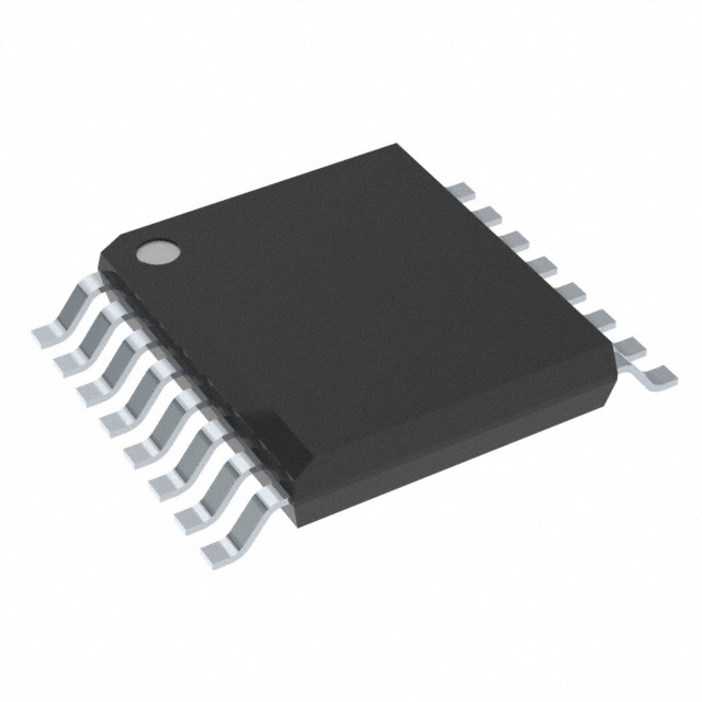
The SN74LVC257ADBR is a high-performance multiplexer integrated circuit (IC) designed by Texas Instruments. This device is part of the 74LVC series, known for its robustness and versatility in digital logic applications. The SN74LVC257ADBR features a 4 x 2:1 multiplexer configuration, enabling it to select between two input signals and route them to a single output. This multiplexer operates on a single supply voltage ranging from 1.65V to 3.6V, making it suitable for a wide range of low-power applications. The device is packaged in a 16-lead small outline package (SSOP) and is available in tape and reel format, facilitating surface-mount assembly processes.
SN74LVC257ADBR Features
- Circuit Configuration: The SN74LVC257ADBR features four independent 2:1 multiplexers, allowing for efficient signal routing and selection. This configuration is ideal for applications requiring multiple signal paths to be managed simultaneously.
- Single Supply Operation: With a supply voltage range of 1.65V to 3.6V, the SN74LVC257ADBR is designed for low-power applications, ensuring energy efficiency and compatibility with modern electronic systems.
- High Output Current: The device supports an output current of 24mA for both high and low states, ensuring robust signal integrity and compatibility with a variety of downstream components.
- Surface-Mount Compatibility: The 16SSOP package is designed for surface-mount technology (SMT), enabling automated assembly processes and reducing the overall footprint on printed circuit boards (PCBs).
- Compliance and Reliability: The SN74LVC257ADBR is REACH unaffected and RoHS3 compliant, ensuring it meets environmental and safety standards. Additionally, it has a moisture sensitivity level (MSL) of 1, making it suitable for a wide range of manufacturing environments.
- Active Product Status: As an active product, the SN74LVC257ADBR is readily available and supported by Texas Instruments, ensuring long-term availability and technical support.
SN74LVC257ADBR Applications
The SN74LVC257ADBR is well-suited for a variety of applications, particularly those requiring efficient signal routing and selection. Some specific use cases include:
- Data Communication Systems: In systems where multiple data sources need to be selectively routed to a single output, the SN74LVC257ADBR provides a reliable and efficient solution.
- Digital Signal Processing: The multiplexer can be used to switch between different digital signals, enabling flexible signal processing architectures.
- Automotive Electronics: The device's low-power operation and robustness make it suitable for automotive applications where space and power consumption are critical.
- Industrial Control Systems: The SN74LVC257ADBR can be used to manage multiple sensor inputs or control signals, enhancing the flexibility and functionality of industrial control systems.
Conclusion of SN74LVC257ADBR
The SN74LVC257ADBR is a versatile and reliable multiplexer IC that offers significant advantages over similar models. Its wide supply voltage range, high output current, and surface-mount compatibility make it an ideal choice for a variety of applications. The device's compliance with environmental and safety standards ensures it meets the requirements of modern electronics manufacturing. Whether used in data communication systems, digital signal processing, automotive electronics, or industrial control systems, the SN74LVC257ADBR provides a robust and efficient solution for signal routing and selection.
FAQ
| Quantity | Unit Price | Ext. Price |
|---|---|---|
| 1+ | $0.54560 | $0.55 |
| 10+ | $0.38456 | $3.85 |
| 25+ | $0.34426 | $8.61 |
| 100+ | $0.30043 | $30.04 |
| 250+ | $0.27952 | $69.88 |
Not available to buy online? Want the lower wholesale price? Please Send RFQ to get best price, we will respond immediately


.png?x-oss-process=image/format,webp/resize,h_32)


