
 German
 Japanese
 Portuguese
 Korea
Korea
 Mexico
 Dutch
Dutch


Texas Instruments
SN74LVC2G06YEPR

Why Choose Us?
Professional Platform
B2B & B2C purchasingDelivery at full speed
1-2 days deliveryWide variety
Original manufacturers365 days guarantee
Responsible quality
.png)


Tech Specifications
SN74LVC2G06YEPR Description
SN74LVC2G06YEPR Description
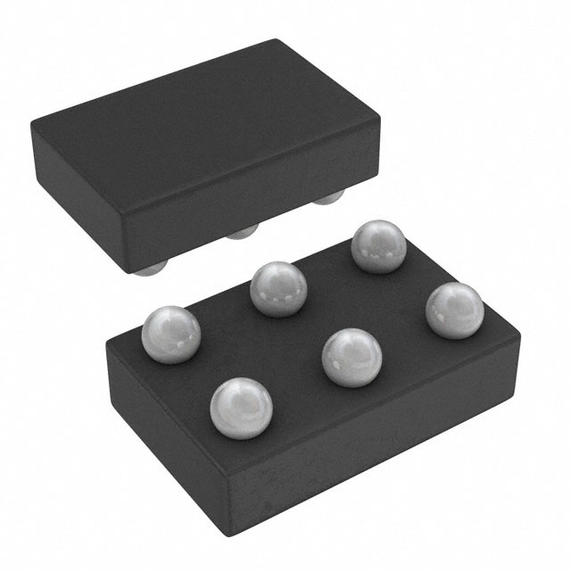
The SN74LVC2G06YEPR is a dual-channel inverter IC designed by Texas Instruments, featuring two independent inverter circuits with open-drain outputs. This logic IC chip is part of the 74LVC series, known for its robust performance and compatibility across a wide range of supply voltages, from 1.65V to 5.5V. The device is housed in a 6-DSBGA package, which is ideal for surface-mount applications, ensuring efficient space utilization on printed circuit boards.
SN74LVC2G06YEPR Features
- Max Propagation Delay: 2.9ns at 5V with a maximum load capacitance of 50pF, ensuring fast signal inversion and minimal delay.
- Input Logic Levels: The input logic levels are well-defined, with a low level ranging from 0.7V to 0.8V and a high level from 1.7V to 2V, providing precise signal handling.
- Open Drain Outputs: The open-drain feature allows for versatile output configurations, enabling the use of pull-up resistors to customize output voltage levels.
- Low Quiescent Current: With a maximum quiescent current of 10 µA, the SN74LVC2G06YEPR is highly energy-efficient, making it suitable for low-power applications.
- RoHS3 Compliant: The device meets the stringent environmental standards of RoHS3, ensuring it is free from hazardous substances.
- REACH Unaffected: The SN74LVC2G06YEPR complies with REACH regulations, indicating it does not contain substances of very high concern.
- Moisture Sensitivity Level (MSL): Rated at MSL 1 (Unlimited), the device is highly resistant to moisture, reducing the risk of damage during manufacturing processes.
- Packaging: Supplied in a Tape & Reel (TR) format, facilitating automated assembly and handling in high-volume production environments.
SN74LVC2G06YEPR Applications
The SN74LVC2G06YEPR is well-suited for a variety of applications due to its versatile features and performance characteristics. Some specific use cases include:
- Digital Signal Processing: Ideal for inverting digital signals in communication systems, microcontrollers, and other digital circuits.
- Power Management: Its low quiescent current and wide supply voltage range make it suitable for power management applications where energy efficiency is critical.
- Automotive Electronics: The device's robustness and compliance with environmental regulations make it suitable for automotive applications, where reliability and environmental compliance are paramount.
- Consumer Electronics: The SN74LVC2G06YEPR can be used in consumer electronics for signal inversion and processing, contributing to the overall performance and functionality of devices.
Conclusion of SN74LVC2G06YEPR
The SN74LVC2G06YEPR is a high-performance dual-channel inverter IC that offers significant advantages over similar models. Its fast propagation delay, precise input logic levels, and open-drain outputs make it suitable for a wide range of applications. The device's compliance with environmental regulations and its robust packaging ensure it is reliable and environmentally friendly. While the product is marked as obsolete, it remains a valuable component for existing designs and applications where its unique features are required.
FAQ
Not available to buy online? Want the lower wholesale price? Please Send RFQ to get best price, we will respond immediately


.png?x-oss-process=image/format,webp/resize,h_32)


