
 German
 Japanese
 Portuguese
 Korea
Korea
 Mexico
 Dutch
Dutch


Texas Instruments
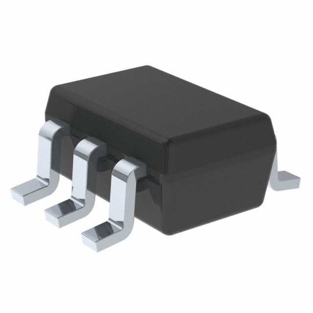
SN74LVC2G17DCK3

Why Choose Us?
Professional Platform
B2B & B2C purchasingDelivery at full speed
1-2 days deliveryWide variety
Original manufacturers365 days guarantee
Responsible quality
.png)


Tech Specifications
SN74LVC2G17DCK3 Description
SN74LVC2G17DCK3 Description
The SN74LVC2G17DCK3 is a high-performance, dual-buffer gate from Texas Instruments, designed to offer reliable signal transmission and buffering capabilities. This device features a Schmitt trigger input type, which helps to eliminate noise and provide stable signal transitions. With a supply voltage range of 1.65V to 5.5V, it is suitable for a wide range of applications requiring low-voltage operation. The SN74LVC2G17DCK3 is RoHS3 compliant, REACH unaffected, and EAR99 classified, ensuring compliance with international regulations.
SN74LVC2G17DCK3 Features
- Schmitt Trigger Input Type: Provides noise immunity and ensures stable signal transitions.
- Dual Buffer Gates: Offers two independent buffer elements for increased flexibility in signal routing and buffering.
- Wide Voltage Range: Operates from 1.65V to 5.5V, making it suitable for low-voltage applications.
- Low Output Current: 32mA high and low output current, ensuring efficient power consumption.
- Surface Mount Technology: Facilitates easy integration into surface mount PCB designs.
- Active Product Status: Ensures ongoing availability and support from Texas Instruments.
- 74LVC Series: Part of the popular 74LVC series, known for its high performance and reliability.
SN74LVC2G17DCK3 Applications
The SN74LVC2G17DCK3 is ideal for a variety of applications where signal buffering and transmission are critical:
- Digital Communication Systems: Used for signal conditioning and buffering in digital communication systems, such as routers and switches.
- Automotive Electronics: Employed in automotive control systems for reliable signal transmission between various electronic control units (ECUs).
- Industrial Control Systems: Utilized in industrial control systems for signal buffering and isolation, ensuring stable and reliable operation.
- Consumer Electronics: Integrated into consumer electronics, such as smartphones and tablets, for signal routing and buffering.
Conclusion of SN74LVC2G17DCK3
The SN74LVC2G17DCK3 from Texas Instruments is a versatile and reliable dual-buffer gate, offering a wide voltage range, Schmitt trigger inputs, and low output current. Its unique features, such as the Schmitt trigger and surface mount technology, make it an ideal choice for applications requiring stable signal transmission and efficient power consumption. With its active product status and compliance with international regulations, the SN74LVC2G17DCK3 is a dependable solution for a variety of digital signal processing and buffering applications.
FAQ
| Quantity | Unit Price | Ext. Price |
|---|---|---|
| 5+ | $0.43391 | $2.17 |
| 50+ | $0.34864 | $17.43 |
| 150+ | $0.31208 | $46.81 |
Not available to buy online? Want the lower wholesale price? Please Send RFQ to get best price, we will respond immediately


.png?x-oss-process=image/format,webp/resize,h_32)


