
 German
 Japanese
 Portuguese
 Korea
Korea
 Mexico
 Dutch
Dutch


Texas Instruments
SN74LVC2G17DCKTG4

Why Choose Us?
Professional Platform
B2B & B2C purchasingDelivery at full speed
1-2 days deliveryWide variety
Original manufacturers365 days guarantee
Responsible quality
.png)


Tech Specifications
SN74LVC2G17DCKTG4 Description
SN74LVC2G17DCKTG4 Description
The SN74LVC2G17DCKTG4 is a high-performance, dual non-inverting buffer IC designed for a wide range of digital applications. Manufactured by Texas Instruments, this device is part of the 74LVC series, known for its robustness and versatility. The SN74LVC2G17DCKTG4 features a Schmitt trigger input type, ensuring stable and reliable operation even with noisy input signals. It operates within a wide supply voltage range of 1.65V to 5.5V, making it suitable for various power supply configurations.
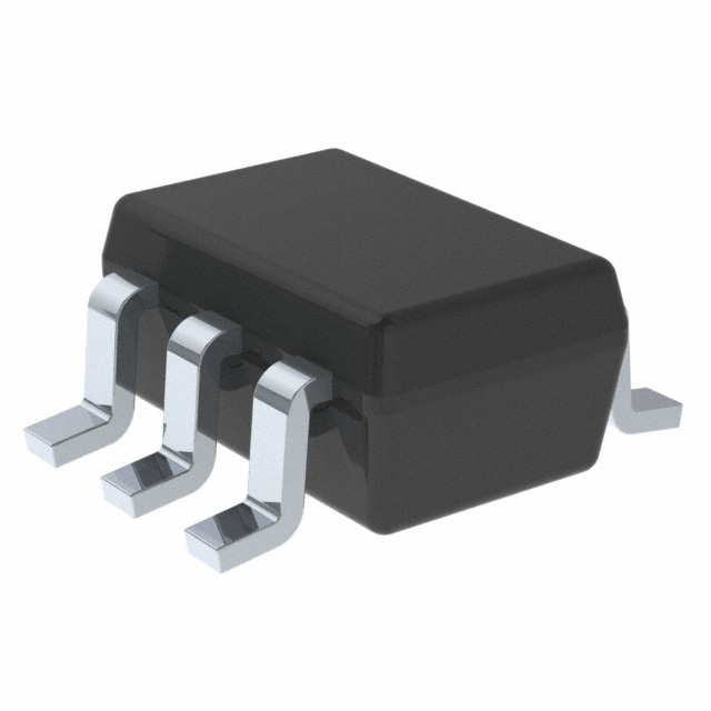
Each of the two buffer elements in the SN74LVC2G17DCKTG4 can handle 1 bit of data, providing efficient signal amplification and conditioning. The device is packaged in a surface-mount SC70-6 package, which is ideal for compact and high-density PCB designs. The SN74LVC2G17DCKTG4 is available in tape and reel packaging, facilitating automated assembly processes and ensuring ease of handling in manufacturing environments.
SN74LVC2G17DCKTG4 Features
- Schmitt Trigger Input: Provides noise immunity and stable operation, making it ideal for applications with noisy input signals.
- Wide Supply Voltage Range: 1.65V to 5.5V ensures compatibility with a variety of power supply systems.
- Dual Non-Inverting Buffers: Each buffer element can handle 1 bit of data, offering efficient signal amplification and conditioning.
- High Output Current: Capable of sourcing and sinking up to 32mA, ensuring robust performance in driving various loads.
- Surface-Mount Packaging: The SC70-6 package is compact and suitable for high-density PCB designs.
- Moisture Sensitivity Level (MSL) 1: Unlimited storage time, reducing the risk of moisture-related issues during manufacturing.
- Compliance: REACH Unaffected and ROHS3 Compliant, ensuring environmental and regulatory standards are met.
- ECCN Classification: EAR99, facilitating international trade and compliance with export regulations.
SN74LVC2G17DCKTG4 Applications
The SN74LVC21G7DCKTG4 is well-suited for a variety of applications due to its robust performance and versatile design. Some specific use cases include:
- Digital Signal Processing: Amplifying and conditioning digital signals in communication systems, ensuring reliable data transmission.
- Consumer Electronics: Enhancing signal integrity in devices such as smartphones, tablets, and IoT devices.
- Automotive Electronics: Providing stable signal buffering in automotive control units and sensor interfaces.
- Industrial Automation: Ensuring reliable operation in harsh industrial environments where noise immunity is critical.
- Medical Devices: Amplifying signals in medical monitoring equipment, where precision and reliability are paramount.
Conclusion of SN74LVC2G17DCKTG4
The SN74LVC2G17DCKTG4 from Texas Instruments is a versatile and reliable dual non-inverting buffer IC. Its Schmitt trigger input and wide supply voltage range make it suitable for a variety of applications, ensuring stable and noise-immune operation. The compact SC70-6 package and surface-mount design facilitate integration into high-density PCBs, while its high output current capability ensures robust performance. Compliance with environmental and regulatory standards further enhances its suitability for modern electronics manufacturing. Whether used in consumer electronics, automotive systems, or industrial applications, the SN74LVC2G17DCKTG4 offers a reliable and efficient solution for digital signal buffering and amplification.
FAQ
Not available to buy online? Want the lower wholesale price? Please Send RFQ to get best price, we will respond immediately


.png?x-oss-process=image/format,webp/resize,h_32)


