

Texas Instruments
SN74LVC4245APWR
Translators, Level Shifters

Not available to buy online? Want the lower wholesale price? Please Send RFQ to get best price, we will respond immediately


- 5+
- $0.18256
- $0.91
- 50+
- $0.14449
- $7.22
- 150+
- $0.12589
- $18.88
- 500+
- $0.10931
- $54.66
- 2000+
- $0.10476
- $209.52
- 4000+
- $0.10203
- $408.12

.png?x-oss-process=image/format,webp/resize,p_30)


SN74LVC4245APWR Description
The SN74LVC4245APWR is a high-speed 3-state octal bus buffer gate with open-drain, non-inverting outputs from Texas Instruments. It is designed to provide efficient and reliable signal buffering and level conversion for various applications.
Description:
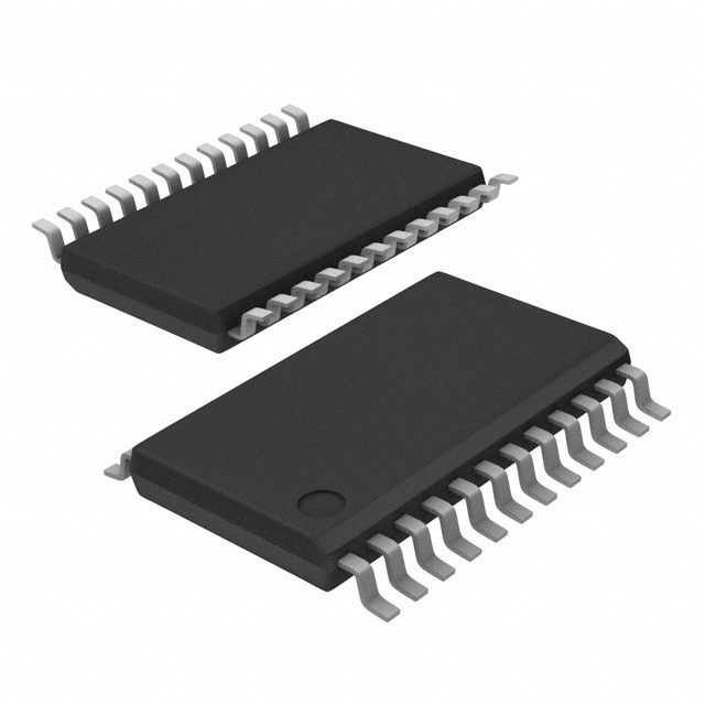
The SN74LVC4245APWR is a member of the 74LVC4245 series, which are high-speed bus buffer gates with open-drain, non-inverting outputs. The device is available in a 20-pin wide SOIC package and operates over a wide supply voltage range of 2.3V to 5.5V.
Features:
- 3-state outputs: The device features 3-state outputs, allowing it to be used in bus applications where multiple devices can share the same data bus.
- Open-drain outputs: The open-drain outputs enable easy interfacing with other open-drain or CMOS devices.
- High-speed performance: The SN74LVC4245APWR offers high-speed operation with a propagation delay of 3.5 ns (typical) and a maximum output rise and fall time of 5 ns (typical).
- Wide supply voltage range: The device operates over a supply voltage range of 2.3V to 5.5V, making it suitable for various applications with different power supply requirements.
- Low power consumption: The SN74LVC4245APWR has a low power consumption of 90 mA maximum for all outputs (typical).
- Non-inverting transfer characteristics: The device provides non-inverting transfer characteristics, ensuring that the output signal is a direct replica of the input signal.
Applications:
- Bus-oriented systems: The 3-state outputs and open-drain design make the SN74LVC4245APWR suitable for bus-oriented systems where multiple devices share the same data bus.
- Signal buffering and level conversion: The high-speed performance and wide supply voltage range make it ideal for buffering and level conversion applications in various digital systems.
- Data bus transceivers: The device can be used as a data bus transceiver in systems requiring bi-directional data communication.
- Microprocessor and memory interfaces: The SN74LVC4245APWR can be used to interface microprocessors with memory devices, providing efficient data transfer and buffering.
- General-purpose buffering: The device can be used for general-purpose buffering applications in digital systems where signal integrity and speed are crucial.
In summary, the SN74LVC4245APWR is a versatile, high-speed bus buffer gate with open-drain, non-inverting outputs that offers efficient signal buffering and level conversion for a wide range of applications, including bus-oriented systems, signal buffering, data bus transceivers, microprocessor and memory interfaces, and general-purpose buffering.
Tech Specifications
SN74LVC4245APWR Documents
Download datasheets and manufacturer documentation for SN74LVC4245APWR
Assembly Site 21/Dec/2022 SN74LVC4245A Datasheet Reels 19/Apr/2018 Reel 10/Jul/2018 SN74LVC4245A Datasheet Mult PN PART MARKING 08/Dec/2023 Related Parts


Shopping Guide


.png?x-oss-process=image/format,webp/resize,h_32)


©2025 ERSA Electronics Corporation.