
 German
 Japanese
 Portuguese
 Korea
Korea
 Mexico
 Dutch
Dutch


Texas Instruments
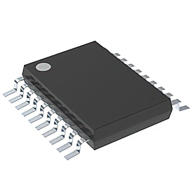
SN74LVC541AQPWREP

Why Choose Us?
Professional Platform
B2B & B2C purchasingDelivery at full speed
1-2 days deliveryWide variety
Original manufacturers365 days guarantee
Responsible quality
.png)


Tech Specifications
SN74LVC541AQPWREP Description
SN74LVC541AQPWREP Description
The SN74LVC541AQPWREP from Texas Instruments is a high-performance, 8-bit non-inverting buffer/driver designed for 2V to 3.6V voltage supply applications. Part of the 74LVC series, this IC is housed in a 20-pin TSSOP package and is available in tape and reel (TR) packaging for automated assembly. It features 24mA output drive strength (both high and low), making it suitable for driving heavy loads in mixed-voltage systems. With RoHS3 compliance and REACH unaffected status, it meets stringent environmental standards. The device operates with a single element (1-channel) and is characterized by low power consumption, making it ideal for portable and battery-powered applications. Its Moisture Sensitivity Level (MSL) 1 rating ensures reliability in humid environments without requiring special handling.
SN74LVC541AQPWREP Features
- 8-bit non-inverting buffer/driver with 3-state outputs for bus-oriented applications.
- Wide operating voltage range (2V–3.6V), compatible with 3.3V and lower-voltage systems.
- High output current (24mA) ensures robust signal integrity in noisy environments.
- Low power consumption with typical CMOS technology advantages.
- ESD protection exceeds 2000V HBM, enhancing durability in harsh conditions.
- Industrial-grade reliability with -40°C to +125°C operating temperature range.
- Tape & reel packaging (TR) for high-volume manufacturing efficiency.
- ROHS3 compliant and REACH unaffected, meeting global environmental regulations.
SN74LVC541AQPWREP Applications
- Bus interface buffering in microcontroller/microprocessor systems.
- Signal conditioning for sensors, memory modules, and FPGAs.
- Level translation between 3.3V and lower-voltage logic families.
- Portable electronics (e.g., smartphones, tablets) due to low power consumption.
- Industrial automation where noise immunity and high drive strength are critical.
- Automotive infotainment systems requiring robust signal integrity.
Conclusion of SN74LVC541AQPWREP
The SN74LVC541AQPWREP stands out as a versatile, high-performance buffer/driver for modern digital systems. Its wide voltage range, high drive capability, and industrial-grade reliability make it superior to basic logic buffers. Ideal for mixed-voltage environments, portable devices, and industrial applications, it combines low power consumption with robust ESD protection. Texas Instruments' reputation for quality ensures this IC is a dependable choice for engineers designing high-speed, noise-immune interfaces. For applications demanding efficiency, durability, and compliance, the SN74LVC541AQPWREP is an optimal solution.
FAQ
| Quantity | Unit Price | Ext. Price |
|---|---|---|
| 1+ | $2.25280 | $2.25 |
| 10+ | $1.67728 | $16.77 |
| 25+ | $1.53296 | $38.32 |
| 100+ | $1.37447 | $137.45 |
| 145+ | $1.81280 | $262.86 |
Not available to buy online? Want the lower wholesale price? Please Send RFQ to get best price, we will respond immediately


.png?x-oss-process=image/format,webp/resize,h_32)


