
 German
 Japanese
 Portuguese
 Korea
Korea
 Mexico
 Dutch
Dutch


Texas Instruments
SN74LVC74AQPWREP

Why Choose Us?
Professional Platform
B2B & B2C purchasingDelivery at full speed
1-2 days deliveryWide variety
Original manufacturers365 days guarantee
Responsible quality
.png)


Tech Specifications
SN74LVC74AQPWREP Description
SN74LVC74AQPWREP Description
The SN74LVC74AQPWREP is a dual D-type flip-flop from Texas Instruments, designed for high-performance digital applications. This device features a clock frequency of up to 150 MHz, making it suitable for high-speed digital systems. It operates within a supply voltage range of 2V to 3.6V, offering flexibility in power supply requirements. The flip-flop is edge-triggered on the positive edge, ensuring reliable and precise data capture.
Each flip-flop element in the SN74LVC74AQPWREP has a single bit of storage, with complementary outputs that provide additional flexibility in circuit design. The device also includes set (preset) and reset functions, which allow for asynchronous control of the flip-flop states. This feature is particularly useful in applications requiring initialization or error recovery mechanisms.
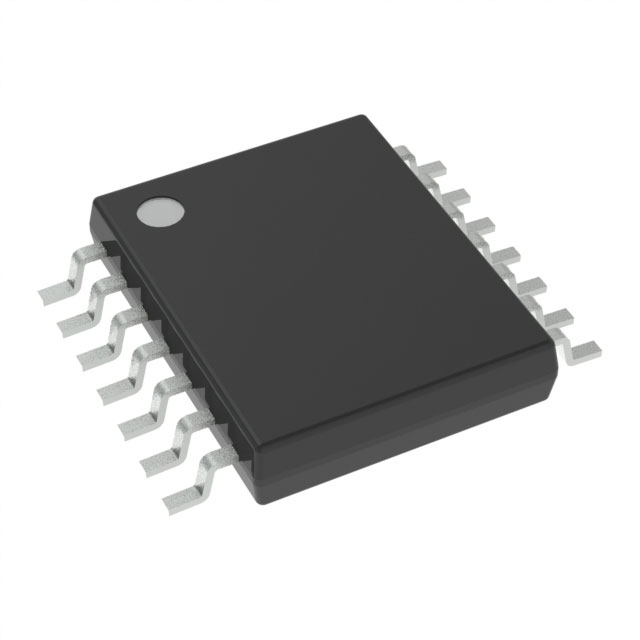
The SN74LVC74AQPWREP is housed in a 14-lead TSSOP package, which is ideal for surface-mount applications. It has an input capacitance of 5 pF, which helps minimize signal propagation delays. The maximum propagation delay is specified as 5.2ns at 3.3V and 50pF, ensuring fast and efficient data transfer. The device draws a quiescent current of only 10 µA, making it energy-efficient for low-power designs.
SN74LVC74AQPWREP Features
- High-Speed Operation: Capable of operating at clock frequencies up to 150 MHz, ensuring high-speed data processing.
- Flexible Power Supply: Operates within a wide voltage range of 2V to 3.6V, providing compatibility with various power supply configurations.
- Edge-Triggered: Positive edge-triggering ensures reliable data capture and synchronization.
- Complementary Outputs: Provides both true and complement outputs, offering additional flexibility in circuit design.
- Set and Reset Functions: Includes asynchronous set (preset) and reset capabilities, allowing for easy initialization and error recovery.
- Low Power Consumption: Draws a quiescent current of only 10 µA, making it suitable for low-power applications.
- Fast Propagation Delay: Achieves a maximum propagation delay of 5.2ns at 3.3V and 50pF, ensuring rapid signal transfer.
- Surface-Mount Package: Available in a 14-lead TSSOP package, ideal for surface-mount technology (SMT) applications.
- Compliance and Safety: REACH unaffected and RoHS3 compliant, ensuring environmental and safety standards are met.
SN74LVC74AQPWREP Applications
The SN74LVC74AQPWREP is well-suited for a variety of high-speed digital applications, including:
- Digital Signal Processing: Ideal for capturing and processing high-speed digital signals in communication systems.
- Clock Management: Used in clock distribution and synchronization circuits to ensure precise timing.
- Data Storage and Transfer: Suitable for temporary data storage and transfer in microprocessors and memory systems.
- Control Logic: Employed in control logic circuits for initializing and resetting system states.
- Consumer Electronics: Used in various consumer electronics devices requiring high-speed data processing and low power consumption.
Conclusion of SN74LVC74AQPWREP
The SN74LVC74AQPWREP from Texas Instruments is a versatile and high-performance dual D-type flip-flop, designed to meet the demands of modern digital systems. Its high-speed operation, flexible power supply, and low power consumption make it an ideal choice for a wide range of applications. The inclusion of set and reset functions, along with complementary outputs, provides additional control and design flexibility. The device's compliance with environmental and safety standards ensures its suitability for use in various industries. Overall, the SN74LVC74AQPWREP offers a reliable and efficient solution for high-speed digital circuit design.
FAQ
| Quantity | Unit Price | Ext. Price |
|---|---|---|
| 1+ | $1.78640 | $1.79 |
| 10+ | $1.32000 | $13.20 |
| 25+ | $1.20243 | $30.06 |
| 100+ | $1.07369 | $107.37 |
| 189+ | $1.39920 | $264.45 |
Not available to buy online? Want the lower wholesale price? Please Send RFQ to get best price, we will respond immediately


.png?x-oss-process=image/format,webp/resize,h_32)


