
 German
 Japanese
 Portuguese
 Korea
Korea
 Mexico
 Dutch
Dutch


Texas Instruments
SN74LVC841ADGVR

Why Choose Us?
Professional Platform
B2B & B2C purchasingDelivery at full speed
1-2 days deliveryWide variety
Original manufacturers365 days guarantee
Responsible quality
.png)


Tech Specifications
SN74LVC841ADGVR Description
SN74LVC841ADGVR Description
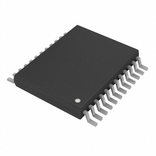
The SN74LVC841ADGVR is a bus-interface latch designed by Texas Instruments, a leading manufacturer in the semiconductor industry. This IC is part of the 74LVC series, known for its robust performance and reliability in various electronic applications. The device is housed in a 24-TVSOP package, which is suitable for surface-mount applications, making it ideal for compact and high-density circuit designs.
The SN74LVC841ADGVR features a 10:10 circuit configuration, meaning it can handle 10 input and 10 output lines, providing efficient data transfer and storage capabilities. It operates within a voltage supply range of 1.65V to 3.6V, ensuring compatibility with a wide range of power supply systems. The device boasts a propagation delay time of 2.7ns, which is remarkably fast and ensures high-speed data processing.
SN74LVC841ADGVR Features
- High-Speed Performance: With a propagation delay of 2.7ns, the SN74LVC841ADGVR ensures rapid data transfer, making it suitable for high-speed applications.
- Wide Voltage Range: The device operates within a voltage range of 1.65V to 3.6V, providing flexibility in power supply requirements.
- High Current Capability: The IC supports an output current of 24mA for both high and low states, enabling robust signal handling.
- Surface-Mount Compatibility: The 24-TVSOP package is designed for surface-mount technology (SMT), allowing for integration into compact and high-density PCB designs.
- Compliance and Safety: The SN74LVC841ADGVR is REACH unaffected and RoHS3 compliant, ensuring it meets environmental and safety standards.
- Low Moisture Sensitivity: With a moisture sensitivity level (MSL) of 1 (unlimited), the device is suitable for storage and handling in various environmental conditions without the need for special precautions.
SN74LVC841ADGVR Applications
The SN74LVC841ADGVR is ideal for applications requiring efficient data latching and high-speed data transfer. Some specific use cases include:
- Data Buffering: The device can be used to buffer data between different sections of a system, ensuring smooth data flow and preventing data loss.
- Memory Interface: It can interface with memory modules, providing a reliable and efficient means of data storage and retrieval.
- Bus Management: The IC is well-suited for managing data buses in complex electronic systems, ensuring data integrity and efficient communication between components.
- Industrial Control Systems: The robustness and reliability of the SN74LVC841ADGVR make it suitable for industrial control systems where high-speed data processing and storage are critical.
Conclusion of SN74LVC841ADGVR
The SN74LVC841ADGVR is a high-performance bus-interface latch that offers a combination of speed, flexibility, and reliability. Its fast propagation delay, wide voltage range, and high current capability make it a versatile component for various electronic applications. The device's surface-mount packaging and compliance with environmental standards further enhance its appeal for modern circuit designs. While the product is now obsolete, its legacy and the benefits it provided during its production run are still noteworthy in the field of logic IC chips.
FAQ
Not available to buy online? Want the lower wholesale price? Please Send RFQ to get best price, we will respond immediately


.png?x-oss-process=image/format,webp/resize,h_32)


