
 German
 Japanese
 Portuguese
 Korea
Korea
 Mexico
 Dutch
Dutch


Texas Instruments
SN74LVC841ADWR

Why Choose Us?
Professional Platform
B2B & B2C purchasingDelivery at full speed
1-2 days deliveryWide variety
Original manufacturers365 days guarantee
Responsible quality
.png)


Tech Specifications
SN74LVC841ADWR Description
SN74LVC841ADWR Description
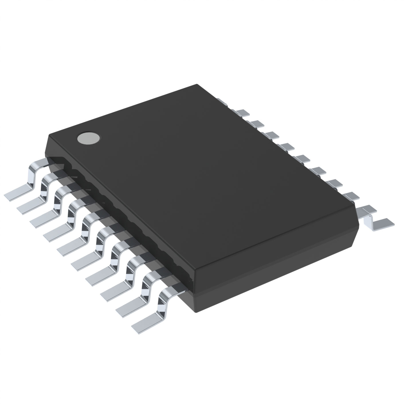
The SN74LVC841ADWR is a 10-bit bus interface D-type latch designed by Texas Instruments, part of the 74LVC series. This device is ideal for applications requiring high-speed data latching and buffering. It features a 10:10 circuit configuration, meaning it has 10 independent input and output lines, each capable of handling digital signals efficiently. The device operates within a supply voltage range of 1.65V to 3.6V, making it suitable for a variety of power supply environments. It is housed in a 24-SOIC package and is available in a tape and reel format, which is ideal for automated surface-mount assembly processes.
SN74LVC841ADWR Features
- High-Speed Performance: With a propagation delay time of 2.7ns, the SN74LVC841ADWR ensures rapid signal transmission and latching, making it suitable for high-speed digital systems.
- Robust Output Current: The device can handle an output current of 24mA for both high and low states, providing strong drive capabilities for interfacing with various digital circuits.
- Wide Operating Voltage Range: The 1.65V to 3.6V supply voltage range offers flexibility in power supply design, allowing compatibility with different system architectures.
- Surface-Mount Compatibility: The surface-mount package type facilitates easy integration into modern printed circuit board (PCB) designs, enhancing reliability and reducing the overall footprint.
- Compliance and Safety: The SN74LVC841ADWR is REACH unaffected and ROHS3 compliant, ensuring it meets environmental and safety standards. It also has a moisture sensitivity level (MSL) of 1, indicating unlimited shelf life under standard conditions.
- Independent Circuits: Each of the 10 channels operates independently, allowing for versatile data handling and minimizing the risk of signal interference.
SN74LVC841ADWR Applications
The SN74LVC841ADWR is well-suited for a range of applications where reliable data latching and buffering are critical. Some specific use cases include:
- Data Processing Systems: In high-speed data processing environments, the device can be used to temporarily store data bits, ensuring data integrity during transfer operations.
- Communication Interfaces: It can serve as a buffer in communication protocols, such as SPI or I2C, where data needs to be synchronized between different clock domains.
- Memory Systems: The 10-bit latch can be employed in memory systems to hold data temporarily before it is written to or read from memory modules.
- Industrial Control Systems: In industrial automation, the SN74LVC841ADWR can manage data signals in control systems, ensuring accurate and timely processing of control commands.
Conclusion of SN74LVC841ADWR
The SN74LVC841ADWR, despite being marked as obsolete, remains a valuable component in the electronics industry due to its robust performance and versatile features. Its high-speed operation, wide voltage range, and strong output current capabilities make it an excellent choice for applications requiring reliable data latching and buffering. While newer alternatives may exist, the SN74LVC841ADWR continues to offer a reliable and cost-effective solution for many existing and legacy systems.
FAQ
Not available to buy online? Want the lower wholesale price? Please Send RFQ to get best price, we will respond immediately


.png?x-oss-process=image/format,webp/resize,h_32)


