

Texas Instruments
SN74LVCU04ADBR
Gates and Inverters

Not available to buy online? Want the lower wholesale price? Please Send RFQ to get best price, we will respond immediately


.png?x-oss-process=image/format,webp/resize,p_30)


SN74LVCU04ADBR Description
SN74LVCU04ADBR Description
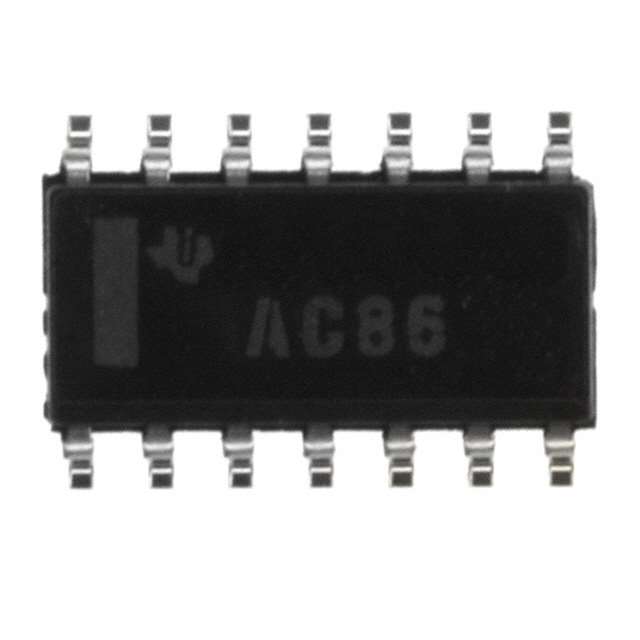
The SN74LVCU04ADBR is a high-performance, 6-channel inverter IC designed for a wide range of digital logic applications. Manufactured by Texas Instruments, this device is part of the 74LVCU series and is packaged in a 14-lead small outline package (14SSOP). It is specifically engineered to provide robust performance with low power consumption and high-speed operation.
SN74LVCU04ADBR Features
- Logic Type: The SN74LVCU04ADBR is an inverter, which means it performs logical negation on the input signal, converting a high input to a low output and vice versa. This makes it ideal for signal inversion and level shifting in digital circuits.
- Supply Voltage Range: It operates within a wide supply voltage range of 1.65V to 3.6V, making it suitable for various power supply configurations and ensuring compatibility with different digital systems.
- Max Propagation Delay: With a maximum propagation delay of 3.8ns at 3.3V and 50pF load capacitance, the SN74LVCU04ADBR ensures fast signal processing and minimal delay, crucial for high-speed digital applications.
- Input Logic Levels: The device supports input logic levels of 0.4V to 0.65V for low and 1.32V to 2.88V for high, providing flexibility and compatibility with different digital logic families.
- Output Current: It can source and sink up to 24mA, making it capable of driving multiple loads and ensuring reliable signal transmission.
- Low Quiescent Current: The maximum quiescent current of 10 µA ensures minimal power consumption, making it suitable for low-power applications.
- Compliance and Packaging: The SN74LVCU04ADBR is REACH unaffected and RoHS3 compliant, adhering to environmental and safety standards. It is available in a tape and reel (TR) package, facilitating easy handling and assembly in automated manufacturing processes.
- Moisture Sensitivity Level: With an MSL of 1 (Unlimited), the device is highly resistant to moisture, ensuring reliability in various environmental conditions.
SN74LVCU04ADBR Applications
The SN74LVCU04ADBR is versatile and finds applications in a variety of electronic systems, including:
- Digital Signal Processing: Ideal for inverting and processing digital signals in communication systems, microcontrollers, and digital signal processors.
- Level Shifting: Used to convert signal levels between different digital systems, ensuring compatibility preventing and signal degradation.
- Clock Signal Inversion: In digital circuits where clock signals need to be inverted for synchronization and timing purposes.
- Data Buffering: Acts as a buffer to drive multiple loads, ensuring signal integrity and reducing the load on the driving circuit.
- Consumer Electronics: Suitable for applications in consumer electronics where low power consumption and high performance are critical.
Conclusion of SN74LVCU04ADBR
The SN74LVCU04ADBR is a reliable and efficient inverter IC that offers high performance and flexibility. Its wide supply voltage range, low propagation delay, and robust output current capabilities make it an excellent choice for a variety of digital applications. The device's compliance with environmental standards and its moisture resistance further enhance its reliability and suitability for diverse operating conditions. Whether used in digital signal processing, level shifting, or data buffering, the SN74LVCU04ADBR stands out as a superior solution in the electronics industry.
Tech Specifications
SN74LVCU04ADBR Documents
Download datasheets and manufacturer documentation for SN74LVCU04ADBR
SN74LVCU04A SN74LVCU04A Related Parts


Shopping Guide


.png?x-oss-process=image/format,webp/resize,h_32)


©2025 ERSA Electronics Corporation.