

Texas Instruments
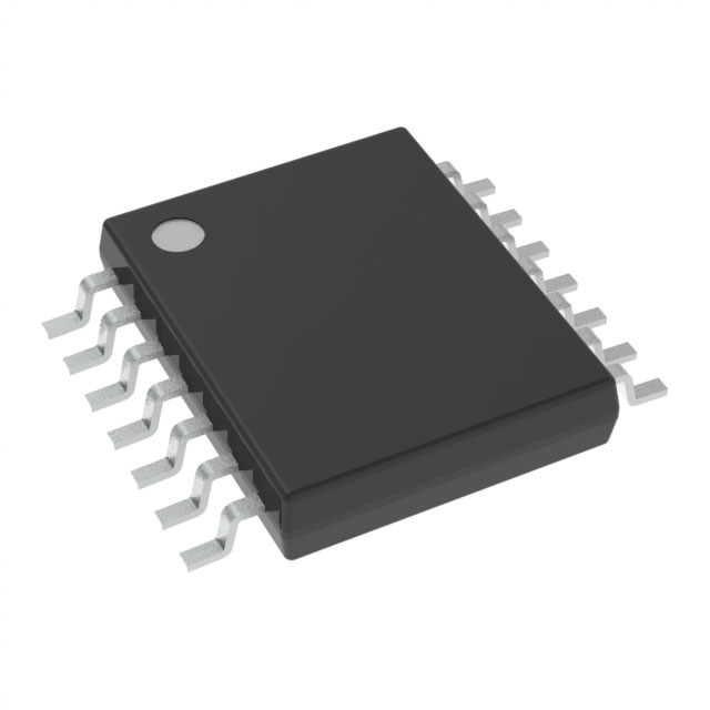
SN74LVCU04APWT
Gates and Inverters

Not available to buy online? Want the lower wholesale price? Please Send RFQ to get best price, we will respond immediately


.png?x-oss-process=image/format,webp/resize,p_30)


SN74LVCU04APWT Description
SN74LVCU04APWT Description
The SN74LVCU04APWT is a high-performance inverter logic IC chip designed by Texas Instruments. It belongs to the 74LVCU series and is housed in a 14-TSSOP package. This device features six inverter circuits, each with a single input, making it suitable for a variety of digital logic applications. The SN74LVCU04APWT operates within a supply voltage range of 1.65V to 3.6V and supports a maximum propagation delay of 3.8ns at 3.3V with a load capacitance of 50pF. It has a maximum quiescent current of 10 µA and can handle output currents of up to 24mA for both high and low states. The input logic levels are specified as 0.4V to 0.65V for low and 1.32V to 2.88V for high, ensuring compatibility with a wide range of digital systems. The device is RoHS3 compliant and REACH unaffected, making it suitable for environmentally conscious applications. It is also available in a surface-mount package, which is ideal for automated assembly processes. Despite being marked as obsolete, the SN74LVCU04APWT remains a reliable choice for legacy systems and specific applications where its unique features are required.
SN74LVCU04APWT Features
- High-Speed Performance: With a maximum propagation delay of 3.8ns at 3.3V and 50pF load capacitance, the SN74LVCU04APWT ensures fast signal processing and minimal latency, making it ideal for high-speed digital circuits.
- Wide Operating Voltage Range: The device operates within a supply voltage range of 1.65V to 3.6V, providing flexibility in power supply design and compatibility with various digital systems.
- Low Quiescent Current: A maximum quiescent current of 10 µA ensures minimal power consumption, making it suitable for low-power and battery-operated applications.
- Robust Output Current Capability: The SN74LVCU04APWT can handle output currents of up to 24mA for both high and low states, ensuring reliable signal transmission and driving capabilities.
- Surface-Mount Packaging: The 14-TSSOP package is designed for surface-mount technology, facilitating automated assembly and reducing board space requirements.
- Environmental Compliance: The device is RoHS3 compliant and REACH unaffected, making it suitable for environmentally conscious applications and ensuring compliance with global regulations.
- Single Input Inverter Circuits: Each of the six inverter circuits features a single input, simplifying design and reducing complexity in digital logic applications.
SN74LVCU04APWT Applications
The SN74LVCU04APWT is well-suited for a variety of applications where high-speed digital signal processing and inversion are required. Some specific use cases include:
- Digital Signal Processing: The fast propagation delay and robust output current capability make it ideal for processing and inverting digital signals in communication systems and data processing applications.
- Automotive Electronics: The wide operating voltage range and low quiescent current ensure reliable operation in automotive environments where power supply voltages can vary.
- Consumer Electronics: The device's low power consumption and surface-mount packaging make it suitable for consumer electronics where space and power efficiency are critical.
- Industrial Control Systems: The robust output current capability and environmental compliance make it suitable for industrial applications where reliability and compliance with regulations are essential.
- Legacy Systems: Despite being marked as obsolete, the SN74LVCU04APWT remains a reliable choice for maintaining and upgrading legacy systems where its unique features and compatibility are required.
Conclusion of SN74LVCU04APWT
The SN74LVCU04APWT is a versatile and high-performance inverter logic IC chip designed for a wide range of digital logic applications. Its fast propagation delay, wide operating voltage range, and low quiescent current make it an ideal choice for high-speed digital signal processing and inversion. The device's robust output current capability, surface-mount packaging, and environmental compliance further enhance its suitability for modern electronic systems. Although marked as obsolete, the SN74LVCU04APWT remains a reliable and efficient solution for specific applications where its unique features are required.
Tech Specifications
SN74LVCU04APWT Documents
Download datasheets and manufacturer documentation for SN74LVCU04APWT
SN74LVCU04A SN74LVCU04A Related Parts


Shopping Guide


.png?x-oss-process=image/format,webp/resize,h_32)


©2025 ERSA Electronics Corporation.