
 German
 Japanese
 Portuguese
 Korea
Korea
 Mexico
 Dutch
Dutch


Texas Instruments
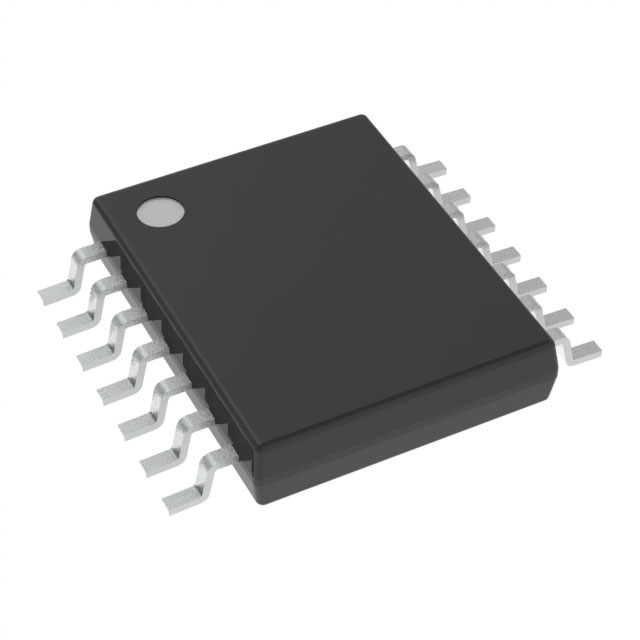
SN74LVTH125PW

Why Choose Us?
Professional Platform
B2B & B2C purchasingDelivery at full speed
1-2 days deliveryWide variety
Original manufacturers365 days guarantee
Responsible quality
.png)


Tech Specifications
SN74LVTH125PW Description
SN74LVTH125PW Description
The SN74LVTH125PW from Texas Instruments is a high-performance quad bus buffer gate designed for 3.3V VCC operation, featuring non-inverting outputs and tri-state functionality. Housed in a 14-pin TSSOP package, this device is optimized for low-voltage applications (2.7V to 3.6V) while delivering robust output drive capability (32mA high/64mA low). As part of the 74LVTH series, it combines LVTTL compatibility with 5V-tolerant inputs, making it ideal for mixed-voltage systems. Its surface-mount design and RoHS3 compliance ensure environmental and regulatory suitability for modern electronics.
SN74LVTH125PW Features
- Quad Non-Inverting Buffer: Four independent 1-bit buffers with tri-state outputs for bus isolation.
- Wide Operating Voltage: Supports 2.7V to 3.6V, compatible with 3.3V logic systems.
- High Drive Strength: 32mA (high)/64mA (low) output current for driving heavy loads.
- 5V-Tolerant Inputs: Allows interfacing with 5V logic without external level shifters.
- Low Power Consumption: LVTH technology reduces static and dynamic power dissipation.
- Robust Packaging: 14-TSSOP with MSL1 (Unlimited) moisture sensitivity, suitable for automated assembly.
- Enhanced ESD Protection: Exceeds 2000V HBM for improved reliability.
SN74LVTH125PW Applications
- Bus Buffering: Isolates and drives bus lines in microcontroller/microprocessor systems.
- Mixed-Voltage Systems: Bridges 3.3V and 5V logic in industrial controls or automotive electronics.
- Signal Conditioning: Cleans up noisy signals in sensor interfaces or communication modules.
- Hot-Swap Protection: Tri-state outputs prevent contention during live insertion (backplanes, PCI cards).
- Portable Electronics: Low-voltage operation suits battery-powered devices like IoT nodes or handheld instruments.
Conclusion of SN74LVTH125PW
The SN74LVTH125PW stands out for its high drive strength, voltage flexibility, and robustness, making it a versatile choice for 3.3V logic systems. Its 5V-tolerant inputs and tri-state control simplify design in mixed-voltage environments, while the TSSOP package ensures space efficiency. Ideal for industrial, automotive, and consumer applications, this buffer combines performance with reliability, backed by Texas Instruments' quality assurance.
FAQ
| Quantity | Unit Price | Ext. Price |
|---|---|---|
| 1+ | $0.99440 | $0.99 |
| 10+ | $0.71544 | $7.15 |
| 90+ | $0.57601 | $51.84 |
| 180+ | $0.54702 | $98.46 |
| 270+ | $0.53250 | $143.78 |
Not available to buy online? Want the lower wholesale price? Please Send RFQ to get best price, we will respond immediately


.png?x-oss-process=image/format,webp/resize,h_32)


