
 German
 Japanese
 Portuguese
 Korea
Korea
 Mexico
 Dutch
Dutch


Texas Instruments
SNJ54LS375J

Why Choose Us?
Professional Platform
B2B & B2C purchasingDelivery at full speed
1-2 days deliveryWide variety
Original manufacturers365 days guarantee
Responsible quality
.png)


Tech Specifications
SNJ54LS375J Description
SNJ54LS375J Description
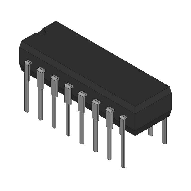
The SNJ54LS375J is a 4-bit bistable latch designed for high-performance digital logic applications. Manufactured by Texas Instruments, this logic IC chip belongs to the 54LS series and is housed in a 16-CDIP package. It features a complementary output type and consists of two independent circuits, each with a 2:2 configuration. The device is designed for through-hole mounting, making it suitable for a variety of printed circuit board (PCB) designs.
SNJ54LS375J Features
- Output Type: Complementary outputs ensure robust signal integrity and compatibility with a wide range of digital systems.
- Independent Circuits: The device includes two independent circuits, providing flexibility and functionality for complex digital designs.
- Voltage Supply: Operates within a supply voltage range of 4.5V to 5.5V, ensuring compatibility with standard TTL logic levels.
- Propagation Delay: With a delay time of 15ns, the SNJ54LS375J offers fast switching capabilities, making it suitable for high-speed digital applications.
- Output Current: The device supports an output current of 400µA for high-level outputs and 8mA for low-level outputs, providing sufficient drive capability for various digital loads.
- Compliance: The SNJ54LS375J is REACH unaffected and RoHS3 compliant, ensuring it meets environmental and regulatory standards for electronic components.
- Packaging: Supplied in a tube package, which facilitates easy handling and storage during manufacturing processes.
- Moisture Sensitivity Level: Not applicable, indicating the device is not susceptible to moisture-related issues during storage or assembly.
SNJ54LS375J Applications
The SNJ54LS375J is ideal for applications requiring reliable and efficient digital signal processing. Its 4-bit bistable latch functionality makes it suitable for:
- Data Storage and Buffering: Ideal for temporary storage and buffering of digital data in microprocessor systems and memory modules.
- Digital Logic Circuits: Can be used in complex digital logic circuits where multiple independent latches are required.
- Control Systems: Suitable for control systems in industrial automation, where reliable and fast signal processing is crucial.
- Communication Systems: Can be employed in communication systems for data synchronization and signal buffering.
Conclusion of SNJ54LS375J
The SNJ54LS375J from Texas Instruments is a versatile and high-performance 4-bit bistable latch designed for a wide range of digital applications. Its complementary output type, independent circuits, and fast propagation delay make it a reliable choice for digital signal processing. The device's compliance with environmental and regulatory standards ensures it meets the requirements of modern electronics manufacturing. With its robust performance and flexibility, the SNJ54LS375J is an excellent choice for engineers and designers looking for a reliable and efficient digital logic solution.
FAQ
| Quantity | Unit Price | Ext. Price |
|---|---|---|
| 15+ | $17.05440 | $255.82 |
Not available to buy online? Want the lower wholesale price? Please Send RFQ to get best price, we will respond immediately


.png?x-oss-process=image/format,webp/resize,h_32)


