
 German
 Japanese
 Portuguese
 Korea
Korea
 Mexico
 Dutch
Dutch



Texas Instruments
SNJ54LS74AFK


Why Choose Us?
Professional Platform
B2B & B2C purchasingDelivery at full speed
1-2 days deliveryWide variety
Original manufacturers365 days guarantee
Responsible quality

.png)



Tech Specifications
SNJ54LS74AFK Description
SNJ54LS74AFK Description
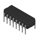
The SNJ54LS74AFK is a dual D-type positive-edge-triggered flip-flop designed for high-speed synchronous operations. Manufactured by Texas Instruments, this logic IC chip belongs to the 54LS series and is optimized for robust performance in a wide range of digital applications. The device features a clock frequency of 33 MHz, ensuring rapid data processing and synchronization. It operates within a supply voltage range of 4.5V to 5.5V, making it suitable for standard TTL logic circuits.
SNJ54LS74AFK Features
- High-Speed Operation: With a maximum propagation delay of 40ns at 5V and 15pF, the SNJ54LS74AFK ensures minimal latency in signal processing.
- Low Power Consumption: The quiescent current is only 8 mA, making it energy-efficient for applications where power consumption is a critical factor.
- Dual Elements: The chip contains two D-type flip-flops, each with a single bit per element, allowing for compact and efficient circuit designs.
- Complementary Outputs: The output type is complementary, providing both true and complement outputs, which enhances flexibility in circuit design.
- Positive Edge Triggering: The flip-flops are triggered on the positive edge of the clock signal, ensuring precise timing control.
- Set and Reset Functionality: The device includes set (preset) and reset functions, enabling dynamic control over the flip-flop states.
- Surface Mount Packaging: The SNJ54LS74AFK is available in a surface mount package, facilitating easy integration into modern PCB designs.
- ROHS3 Compliant: The device meets the stringent environmental standards of ROHS3, ensuring it is free from hazardous substances.
- Wide Operating Voltage Range: The supply voltage range of 4.5V to 5.5V makes it compatible with a variety of power supply configurations.
- High Output Current Capability: The output current capability is 400µA for high output and 4mA for low output, ensuring reliable signal drive strength.
SNJ54LS74AFK Applications
The SNJ54LS74AFK is ideal for a variety of applications where high-speed, reliable, and low-power digital signal processing is required. Some specific use cases include:
- Digital Clock Circuits: The positive-edge-triggered flip-flops are perfect for generating and synchronizing clock signals in digital systems.
- Data Storage and Latching: The set and reset functions, along with the dual flip-flops, make it suitable for data storage and latching applications.
- Frequency Dividers: The device can be used to divide clock frequencies, enabling the creation of sub-clocks for various digital components.
- Counter Circuits: The flip-flops can be cascaded to form binary counters, useful in digital timing and counting applications.
- Synchronization Circuits: The high-speed operation and precise triggering make it ideal for synchronizing data streams in communication systems.
- Memory Circuits: The dual flip-flops can be used in memory circuits to store and retrieve data bits.
Conclusion of SNJ54LS74AFK
The SNJ54LS74AFK from Texas Instruments is a versatile and high-performance dual D-type positive-edge-triggered flip-flop. Its combination of high-speed operation, low power consumption, and robust functionality makes it an excellent choice for a wide range of digital applications. The complementary outputs, set and reset capabilities, and surface mount packaging further enhance its usability and flexibility. Whether used in digital clock circuits, data storage, or synchronization systems, the SNJ54LS74AFK provides reliable and efficient performance, making it a standout choice in the logic IC chip market.
FAQ
Not available to buy online? Want the lower wholesale price? Please Send RFQ to get best price, we will respond immediately








.png?x-oss-process=image/format,webp/resize,h_32)


