
 German
 Japanese
 Portuguese
 Korea
Korea
 Mexico
 Dutch
Dutch


Texas Instruments
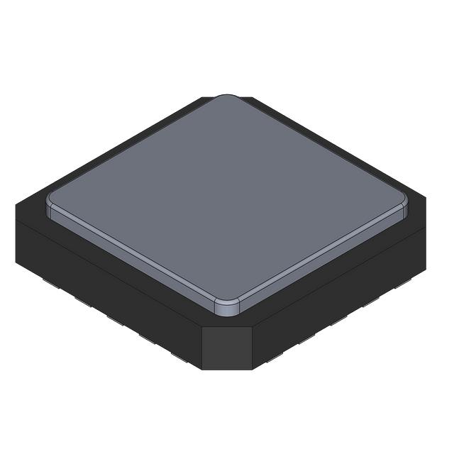
SNJ54LVTH574FK

Why Choose Us?
Professional Platform
B2B & B2C purchasingDelivery at full speed
1-2 days deliveryWide variety
Original manufacturers365 days guarantee
Responsible quality
.png)


Tech Specifications
SNJ54LVTH574FK Description
SNJ54LVTH574FK Description
The SNJ54LVTH574FK is a high-performance, 3.3-V ABT octal edge-triggered D flip-flop designed by Texas Instruments. This device is part of the 54LVTH series and is optimized for high-speed, low-power applications. It features a clock frequency of up to 150 MHz, ensuring rapid data processing and synchronization. The flip-flop operates within a supply voltage range of 2.7V to 3.6V, making it suitable for a variety of power-sensitive designs. With a maximum propagation delay of 4.9ns at 3.3V and 50pF, it delivers exceptional speed and efficiency. The SNJ54LVTH574FK is designed for surface-mount applications, packaged in a tube for easy handling and integration.
SNJ54LVTH574FK Features
- High-Speed Performance: Achieves a clock frequency of up to 150 MHz, enabling rapid data processing.
- Low Propagation Delay: Offers a maximum propagation delay of 4.9ns at 3.3V and 50pF, ensuring quick signal transitions.
- Low Power Consumption: Features a quiescent current of only 190 µA, making it suitable for low-power applications.
- Edge-Triggered Operation: Utilizes positive edge triggering, providing precise control over data latching.
- Robust Output Current: Supports output currents of 24mA for high and 48mA for low, ensuring reliable signal integrity.
- Surface-Mount Compatibility: Designed for surface-mount applications, facilitating easy integration into modern PCB designs.
- RoHS3 Compliant: Meets stringent environmental standards, ensuring compliance with global regulations.
- Wide Operating Voltage Range: Operates within a supply voltage range of 2.7V to 3.6V, offering flexibility in power supply design.
- Low Input Capacitance: With an input capacitance of 3 pF, it minimizes loading effects on driving circuits.
SNJ54LVTH574FK Applications
The SNJ54LVTH574FK is ideal for a range of high-speed, low-power applications, including:
- Digital Signal Processing: Provides fast and reliable data latching for complex digital systems.
- Communication Systems: Ensures precise timing and synchronization in high-speed communication protocols.
- Industrial Control Systems: Offers robust performance in demanding industrial environments.
- Consumer Electronics: Suitable for applications requiring low power consumption and high-speed operation.
- Automotive Electronics: Meets the stringent requirements of automotive applications, ensuring reliability and performance.
Conclusion of SNJ54LVTH574FK
The SNJ54LVTH574FK from Texas Instruments stands out as a high-performance, low-power solution for applications requiring fast and reliable data processing. Its combination of high clock frequency, low propagation delay, and low power consumption makes it an ideal choice for modern electronic designs. The device's edge-triggered operation and robust output current capabilities further enhance its performance and reliability. With its surface-mount compatibility and RoHS3 compliance, the SNJ54LVTH574FK is well-suited for a wide range of applications, from digital signal processing to automotive electronics.
FAQ
| Quantity | Unit Price | Ext. Price |
|---|---|---|
| 5+ | $55.92400 | $279.62 |
Not available to buy online? Want the lower wholesale price? Please Send RFQ to get best price, we will respond immediately


.png?x-oss-process=image/format,webp/resize,h_32)


