Texas Instruments_THS2630SDGKR

Texas Instruments
THS2630SDGKR  
OP Amps, Buffer Amps ICs

Texas Instruments
THS2630SDGKR
687-THS2630SDGKR
Ersa
Texas Instruments-THS2630SDGKR-datasheets-7484364.pdf
IC
In Stock : 2287

Not available to buy online? Want the lower wholesale price? Please Send RFQ to get best price, we will respond immediately

QUICK RFQ
ADD TO RFQ LIST
ersa FreeSample ersa flow
ISO9001
Quality Policy
ISO45001
ISO14001

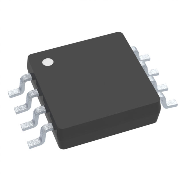
THS2630SDGKR Description

This electronic component uses Tape & Reel (TR) in a way that fits its particular properties. The packaging strategy used for this "THS2630SDGKR" is one of the most popular and affordable packaging options for your company. The manufacturer decides to start mass producing this THS2630SDGKR. The goal of this Texas Instruments is to give its downstream producers to give original and genuine electrical components. This Texas Instruments belongs to OP Amps, Buffer Amps ICs category and it is a portion of the linear IC chips. A linear integrated circuit is a solid-state analog device. It characterizes by a theoretically infinite number of possible operating states. It operates over a continuous range of input levels. Both radio frequency (RF) and audio frequency (AF) amplifiers use this THS2630SDGKR linear integrated circuit. In these applications, the operational amplifier (op amp) is a typical component. The temperature sensor is another typical use for an analog integrated circuit.

Tech Specifications

Voltage - Supply Span (Max)
Number of Channels per Chip
Power Supply Type
Maximum Supply Voltage Range (V)
Maximum Input Offset Voltage (mV)
Maximum Voltage Gain (dB)
Typical Output Current (mA)
PPAP
Gain Bandwidth Product
Product Status
Current - Input Bias
Automotive
Supplier Package
Package / Case
Maximum Operating Supply Voltage (V)
EU RoHS
Amplifier Type
Maximum Dual Supply Voltage (V)
Operating Temperature
Mounting Type
Current - Supply
Standard Package Name
Pin Count
Mounting
Minimum Single Supply Voltage (V)
Minimum PSRR (dB)
Typical Dual Supply Voltage (V)
Voltage - Supply Span (Min)
SVHC
Package
Maximum Input Resistance (MOhm)
Current - Output / Channel
Minimum CMRR (dB)
PCB changed
Output Type
HTS
Number of Elements per Chip
ECCN (US)
Supplier Device Package
Minimum CMRR Range (dB)
Minimum Operating Temperature (°C)
Maximum Operating Temperature (°C)
Typical Gain Bandwidth Product (MHz)
Package Height
Mfr
Typical Single Supply Voltage (V)
Maximum Input Bias Current (uA)
-3db Bandwidth
Slew Rate
Package Length
Minimum Dual Supply Voltage (V)
Voltage - Input Offset
Series
Type
Maximum Single Supply Voltage (V)
Maximum Voltage Gain Range (dB)
Part Status
Number of Circuits
Package Width
Mounting Style
PSRR - Power Supply Rejection Ratio
Gain V/V
Vos - Input Offset Voltage
ECCN
Product
Settling Time
RoHS
Supply Voltage - Min
Minimum Operating Temperature
CMRR - Common Mode Rejection Ratio
Ios - Input Offset Current
Shutdown
SR - Slew Rate
Number of Channels
Maximum Input Resistance
Maximum Operating Temperature
Ib - Input Bias Current
Supply Voltage - Max
USHTS
GBP - Gain Bandwidth Product

THS2630SDGKR Documents

Download datasheets and manufacturer documentation for THS2630SDGKR

Ersa THS2630      

Shopping Guide

Payment Methods
Payment Methods include Prepayment TT (bank transfer), Western Union, and PayPal. Customers are responsible for shipping costs, bank charges, customs duties and taxes.
Shipping Rate
Shipments are made once a day around 5pm, excluding Sundays. Once shipped, the estimated delivery time is usually 5-7 business days, depending on the courier you choose.
Delivery Methods
Provide DHL, FedEx, UPS, EMS, SF Express and Registered Airmail International Delivery Service