
 German
 Japanese
 Portuguese
 Korea
Korea
 Mexico
 Dutch
Dutch


Texas Instruments
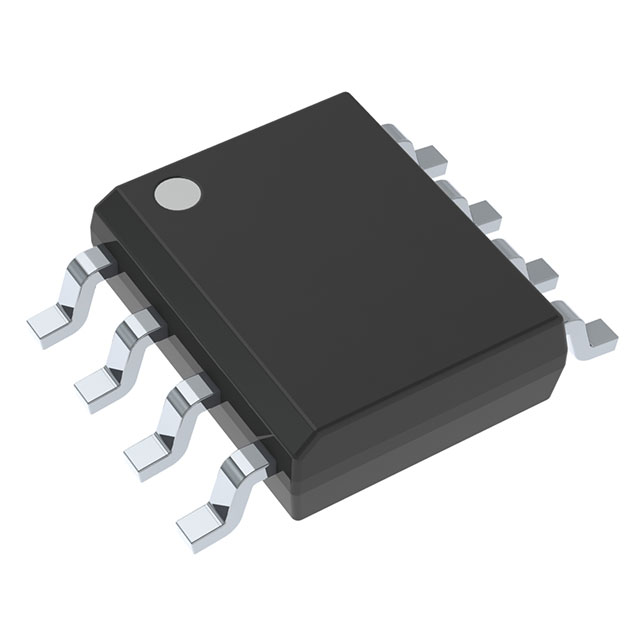
THS3111CDR

Why Choose Us?
Professional Platform
B2B & B2C purchasingDelivery at full speed
1-2 days deliveryWide variety
Original manufacturers365 days guarantee
Responsible quality
.png)


Tech Specifications
THS3111CDR Description
THS3111CDR Description
The THS3111CDR is a high-performance, current feedback operational amplifier (op-amp) designed for demanding applications requiring wide bandwidth and high slew rates. Manufactured by Texas Instruments, this device is part of the Linear IC Chips category and is packaged in an 8-SOIC format suitable for surface mount applications. The THS3111CDR is ideal for a variety of applications due to its robust performance characteristics and compliance with industry standards.
THS3111CDR Features
- Wide Supply Voltage Range: The THS3111CDR operates over a supply voltage range of 10 V to 30 V, making it suitable for a wide range of power supply configurations.
- High Bandwidth and Slew Rate: With a -3 dB bandwidth of 100 MHz and a slew rate of 1300 V/µs, the THS3111CDR excels in high-frequency applications, providing fast response times and minimal signal distortion.
- Low Input Bias Current: The low input bias current of 1.5 µA ensures minimal loading on the input signal source, preserving signal integrity.
- Low Input Offset Voltage: An input offset voltage of 3 mV ensures accurate signal amplification, reducing errors in precision applications.
- High Output Current: The device can deliver up to 260 mA per channel, making it suitable for driving high-current loads.
- Compliance and Reliability: The THS3111CDR is REACH unaffected and ROHS3 compliant, ensuring environmental and regulatory compliance. Additionally, its moisture sensitivity level (MSL) of 1 (unlimited) makes it highly reliable in various environmental conditions.
- Operating Temperature Range: The THS3111CDR operates reliably within a temperature range of 0°C to 70°C, making it suitable for a wide range of industrial and consumer applications.
THS3111CDR Applications
The THS3111CDR is well-suited for applications that demand high performance and reliability. Some specific use cases include:
- High-Speed Signal Processing: Ideal for applications requiring fast signal processing, such as in communication systems, radar, and high-speed data acquisition systems.
- Precision Amplification: Suitable for precision instrumentation where low offset voltage and high slew rate are critical for accurate signal amplification.
- High-Current Drive Applications: The high output current capability makes it suitable for driving actuators, motors, and other high-current loads.
- Wide Bandwidth Applications: The 100 MHz bandwidth makes it suitable for wideband signal processing, ensuring minimal signal degradation at high frequencies.
Conclusion of THS3111CDR
The THS3111CDR from Texas Instruments is a versatile and high-performance current feedback operational amplifier that offers a combination of wide bandwidth, high slew rate, and low input bias current. Its robust performance characteristics, compliance with industry standards, and reliability make it an excellent choice for a variety of demanding applications. Whether used in high-speed signal processing, precision amplification, or high-current drive applications, the THS3111CDR delivers exceptional performance and reliability, setting it apart from similar models in the market.
FAQ
Not available to buy online? Want the lower wholesale price? Please Send RFQ to get best price, we will respond immediately


.png?x-oss-process=image/format,webp/resize,h_32)


