
 German
 Japanese
 Portuguese
 Korea
Korea
 Mexico
 Dutch
Dutch


Texas Instruments
THS4032MDGNREP

Why Choose Us?
Professional Platform
B2B & B2C purchasingDelivery at full speed
1-2 days deliveryWide variety
Original manufacturers365 days guarantee
Responsible quality
.png)


Tech Specifications
THS4032MDGNREP Description
THS4032MDGNREP Description
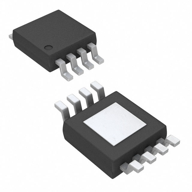
The THS4032MDGNREP from Texas Instruments is a high-performance, dual-channel voltage feedback operational amplifier designed for precision applications requiring wide bandwidth and low distortion. Packaged in an 8-pin HVSSOP and supplied in Tape & Reel (TR), this IC operates over a 9V to 32V supply range, making it versatile for both industrial and automotive systems. With a 200 MHz gain bandwidth product (GBW), 100V/µs slew rate, and 100 MHz -3dB bandwidth, it delivers exceptional signal fidelity for high-speed analog circuits. The device exhibits low input bias current (3 µA) and moderate offset voltage (500 µV), ensuring accuracy in sensitive designs. Its ROHS3 compliance and REACH unaffected status further enhance its suitability for environmentally conscious applications.
THS4032MDGNREP Features
- High-Speed Performance: 200 MHz GBW and 100V/µs slew rate enable rapid signal processing.
- Dual-Channel Design: Integrates two independent amplifiers, reducing board space.
- Wide Supply Range: Supports 9V to 32V, ideal for mixed-voltage systems.
- Low Power Consumption: 7.5mA per channel balances speed and efficiency.
- Robust Output Drive: 90 mA output current per channel for driving capacitive loads.
- Surface-Mount Package: 8-pin HVSSOP ensures compact PCB integration.
- Environmental Compliance: ROHS3 and REACH unaffected, meeting global standards.
THS4032MDGNREP Applications
- Test & Measurement Equipment: High-speed signal conditioning and data acquisition.
- Medical Imaging Systems: Low-noise amplification for sensitive sensors.
- Industrial Automation: Precision control loops and motor drivers.
- Communications Infrastructure: RF and IF signal processing in transceivers.
- Automotive Electronics: ADAS and infotainment systems requiring robust performance.
Conclusion of THS4032MDGNREP
The THS4032MDGNREP stands out as a reliable, high-speed op-amp for demanding applications, combining wide bandwidth, low distortion, and flexible supply options. Its dual-channel integration and environmental compliance make it a preferred choice for engineers designing next-generation industrial, medical, and automotive systems. For projects requiring precision, speed, and durability, this amplifier delivers a competitive edge over similar models.
FAQ
Not available to buy online? Want the lower wholesale price? Please Send RFQ to get best price, we will respond immediately


.png?x-oss-process=image/format,webp/resize,h_32)


