
 German
 Japanese
 Portuguese
 Korea
Korea
 Mexico
 Dutch
Dutch


Texas Instruments
THS4150CDGN

Why Choose Us?
Professional Platform
B2B & B2C purchasingDelivery at full speed
1-2 days deliveryWide variety
Original manufacturers365 days guarantee
Responsible quality
.png)


Tech Specifications
THS4150CDGN Description
THS4150CDGN Description
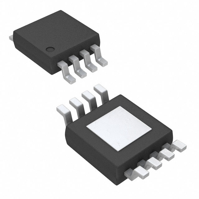
The THS4150CDGN is a high-performance differential operational amplifier designed by Texas Instruments. This IC is part of the OP Amps and Buffer Amps category, offering exceptional performance characteristics suitable for a wide range of applications. The THS4150CDGN features a differential output type, providing a gain bandwidth product of 340 MHz and a -3dB bandwidth of 150 MHz. It operates within a supply voltage range of 4 V to 33 V and offers a high slew rate of 650 V/µs. The amplifier is designed for surface mount applications and comes in an 8HVSSOP package, making it ideal for compact designs.
THS4150CDGN Features
- High Gain Bandwidth Product: The THS4150CDGN boasts a gain bandwidth product of 340 MHz, ensuring high-frequency performance and stability in various applications.
- Differential Output: The differential output type enhances signal integrity and reduces common-mode noise, making it suitable for high-precision applications.
- Wide Supply Voltage Range: With a supply voltage range of 4 V to 33 V, the THS4150CDGN offers flexibility in power supply requirements.
- Low Input Bias Current: The low input bias current of 4.3 µA ensures minimal loading on the input signal source, preserving signal accuracy.
- High Slew Rate: The 650 V/µs slew rate allows for rapid response to input signal changes, making it ideal for high-speed applications.
- Compact Surface Mount Package: The 8HVSSOP package format is ideal for space-constrained designs, providing a balance between performance and footprint.
- Compliance and Reliability: The THS4150CDGN is REACH unaffected and RoHS3 compliant, ensuring environmental safety and regulatory compliance. It also has a moisture sensitivity level (MSL) of 1 (unlimited), making it suitable for various manufacturing environments.
- Operating Temperature Range: The operating temperature range of 0°C to 70°C ensures reliable performance in standard industrial environments.
THS4150CDGN Applications
The THS4150CDGN is well-suited for applications requiring high-speed signal processing and differential signaling. Some specific use cases include:
- High-Speed Data Converters: The high gain bandwidth product and differential output make it ideal for interfacing with high-speed ADCs and DACs.
- Communication Systems: The low input bias current and high slew rate ensure accurate signal transmission in communication systems.
- Medical Imaging: The high precision and differential output are beneficial for medical imaging equipment where signal integrity is critical.
- Industrial Automation: The wide supply voltage range and high operating temperature range make it suitable for industrial automation systems.
- Audio Processing: The high performance and compact package are advantageous for high-fidelity audio processing applications.
Conclusion of THS4150CDGN
The THS4150CDGN from Texas Instruments is a versatile and high-performance differential operational amplifier. Its wide supply voltage range, high gain bandwidth product, and differential output type make it suitable for a variety of applications, from high-speed data conversion to medical imaging. The low input bias current and high slew rate ensure signal integrity and rapid response, while the compact surface mount package and compliance with environmental regulations make it an ideal choice for modern electronic designs. Whether in communication systems, industrial automation, or audio processing, the THS4150CDGN stands out as a reliable and high-performance solution.
FAQ
Not available to buy online? Want the lower wholesale price? Please Send RFQ to get best price, we will respond immediately


.png?x-oss-process=image/format,webp/resize,h_32)


