
Texas Instruments
THS4304DG4
OP Amps, Buffer Amps ICs


.png?x-oss-process=image/format,webp/resize,p_30)


THS4304DG4 Description
THS4304DG4 Description
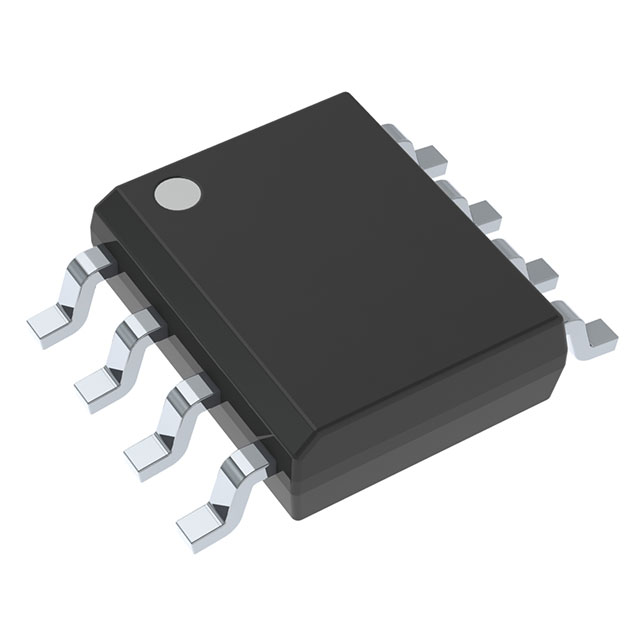
The THS4304DG4 is a high-performance voltage feedback amplifier designed by Texas Instruments. This single-circuit IC is housed in an 8SOIC package, making it suitable for surface mount applications. It operates within a supply voltage range of 2.7 V to 5 V, providing flexibility in power supply design. The THS4304DG4 boasts a gain bandwidth product of 870 MHz and a -3 dB bandwidth of 3 GHz, making it ideal for high-frequency applications. With a slew rate of 830 V/µs, this amplifier ensures fast signal transitions and minimal distortion. The input bias current is low at 7 µA, and the input offset voltage is maintained at 500 µV, contributing to its high precision and stability. The supply current is rated at 18 mA, ensuring efficient power usage. The THS4304DG4 is REACH unaffected and RoHS3 compliant, meeting environmental and safety standards. It also has a moisture sensitivity level (MSL) of 1, indicating unlimited storage conditions without degradation. The ECCN classification is EAR99, and the HTSUS code is 8542.33.0001.
THS4304DG4 Features
The THS4304DG4 features a combination of high performance and efficiency, making it a standout choice in its category. Key features include:
- High Gain Bandwidth Product: With a gain bandwidth product of 870 MHz, the THS4304DG4 can handle high-frequency signals with ease, ensuring minimal phase distortion and excellent signal integrity.
- Wide Supply Voltage Range: The ability to operate between 2.7 V and 5 V supply voltages provides design flexibility, making it suitable for a variety of power supply configurations.
- Low Input Bias Current: The 7 µA input bias current ensures minimal loading on the input signal source, preserving signal quality and reducing noise.
- High Slew Rate: A slew rate of 830 V/µs allows for rapid signal transitions, making it ideal for applications requiring fast response times.
- Low Input Offset Voltage: The 500 µV input offset voltage ensures high precision and accuracy in signal processing.
- Efficient Power Usage: The 18 mA supply current ensures that the amplifier operates efficiently, minimizing power consumption and heat generation.
- Environmental Compliance: The THS4304DG4 is REACH unaffected and RoHS3 compliant, ensuring it meets stringent environmental and safety standards.
- Moisture Sensitivity Level: With an MSL of 1, the THS4304DG4 can be stored in unlimited conditions without risk of moisture damage, enhancing its reliability.
THS4304DG4 Applications
The THS4304DG4 is well-suited for a variety of high-frequency and high-precision applications, including:
- High-Speed Signal Processing: Ideal for applications requiring fast signal transitions and minimal distortion, such as high-speed data acquisition systems and communication interfaces.
- Precision Signal Amplification: Suitable for applications where high precision and low noise are critical, such as precision instrumentation and control systems.
- RF and Microwave Applications: The high gain bandwidth product and wide supply voltage range make it suitable for RF and microwave applications, including radar systems and wireless communication equipment.
- Medical Equipment: The low input bias current and high precision make it ideal for medical equipment where signal integrity and accuracy are paramount.
- Industrial Automation: The robustness and efficiency of the THS4304DG4 make it suitable for industrial automation systems, where reliability and performance are key.
Conclusion of THS4304DG4
The THS4304DG4 from Texas Instruments is a versatile and high-performance voltage feedback amplifier designed to meet the demands of modern electronic systems. Its wide supply voltage range, high gain bandwidth product, and low input bias current make it an excellent choice for high-frequency and high-precision applications. The combination of its high slew rate, low input offset voltage, and efficient power usage ensures that it delivers outstanding performance while maintaining reliability and efficiency. With its environmental compliance and robustness, the THS4304DG4 is a reliable choice for a wide range of applications, from high-speed signal processing to precision instrumentation.
Tech Specifications
THS4304DG4 Documents
Download datasheets and manufacturer documentation for THS4304DG4
 THS4304
  THS4304
 Shopping Guide


.png?x-oss-process=image/format,webp/resize,h_32)


