
 German
 Japanese
 Portuguese
 Korea
Korea
 Mexico
 Dutch
Dutch


Texas Instruments
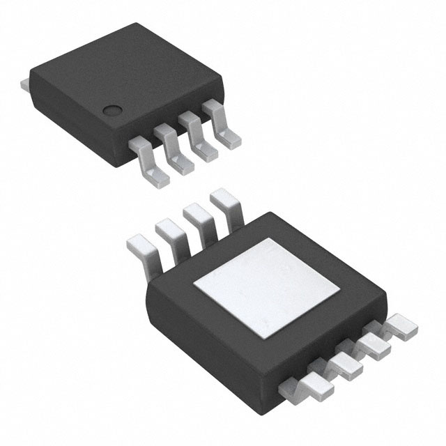
THS4502CDGN

Why Choose Us?
Professional Platform
B2B & B2C purchasingDelivery at full speed
1-2 days deliveryWide variety
Original manufacturers365 days guarantee
Responsible quality
.png)


Tech Specifications
THS4502CDGN Description
THS4502CDGN Description
The THS4502CDGN is a high-performance differential operational amplifier from Texas Instruments, designed for applications requiring exceptional speed and precision. This device features a wide supply voltage range from 4.5 V to 15 V, making it suitable for various power supply configurations. The THS4502CDGN offers a gain bandwidth product of 300 MHz and a -3 dB bandwidth of 370 MHz, ensuring high-frequency performance and fast signal processing capabilities. Its differential output type and a high slew rate of 2800 V/µs make it ideal for applications where accurate and rapid signal transmission is crucial. The amplifier also boasts a low input bias current of 4 µA and an input offset voltage of 1 mV, contributing to its precision and stability.
THS4502CDGN Features
- Wide Supply Voltage Range: Operates from 4.5 V to 15 V, providing flexibility in power supply design.
- High Gain Bandwidth Product: 300 MHz ensures excellent performance in high-frequency applications.
- High Slew Rate: 2800 V/µs allows for rapid signal transitions and minimal distortion.
- Differential Output: Ideal for applications requiring balanced signal transmission.
- Low Input Bias Current: 4 µA minimizes the impact on the input signal source.
- Low Input Offset Voltage: 1 mV ensures high accuracy and stability in signal processing.
- Surface Mount Packaging: The 8HVSSOP package is suitable for compact and high-density PCB designs.
- Compliance and Reliability: ROHS3 compliant and REACH unaffected, ensuring environmental and standards regulatory are met. The moisture sensitivity level (MSL) of 1 (unlimited) ensures robustness in various environmental conditions.
THS4502CDGN Applications
The THS4502CDGN is well-suited for a variety of applications where high-speed and high-precision signal processing is required. Key applications include:
- High-Speed Data Converters: Interfaces with ADCs and DACs to provide fast and accurate signal conditioning.
- Communication Systems: Used in RF and microwave systems for signal amplification and processing.
- Medical Imaging: Enables precise and rapid signal processing in ultrasound and other imaging technologies.
- Industrial Automation: Provides reliable and high-speed signal processing for control systems and sensors.
- Video Signal Processing: Ensures high-quality video signal transmission and processing in professional video equipment.
Conclusion of THS4502CDGN
The THS4502CDGN from Texas Instruments stands out as a versatile and high-performance differential operational amplifier. Its wide supply voltage range, high gain bandwidth product, and high slew rate make it an excellent choice for applications requiring rapid and precise signal processing. The low input bias current and low input offset voltage further enhance its precision and stability. With its surface mount packaging and compliance with environmental and regulatory standards, the THS4502CDGN is a reliable and robust solution for a wide range of high-speed, high-precision applications.
FAQ
Not available to buy online? Want the lower wholesale price? Please Send RFQ to get best price, we will respond immediately


.png?x-oss-process=image/format,webp/resize,h_32)


