

Texas Instruments
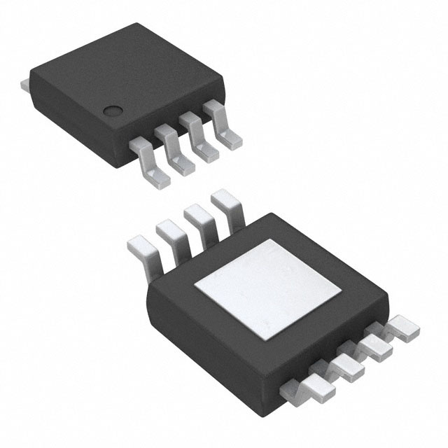
THS4502IDGN
OP Amps, Buffer Amps ICs

Not available to buy online? Want the lower wholesale price? Please Send RFQ to get best price, we will respond immediately


.png?x-oss-process=image/format,webp/resize,p_30)


THS4502IDGN Description
THS4502IDGN Description
The THS4502IDGN is a high-performance differential operational amplifier designed by Texas Instruments, a leading manufacturer in the electronics industry. This device is part of the Linear IC Chips category and is housed in an 8HVSSOP package, making it suitable for surface mount applications. The THS4502IDGN is designed to deliver exceptional performance in terms of bandwidth, slew rate, and power efficiency, making it an ideal choice for a wide range of high-speed analog applications.
THS4502IDGN Features
- High Gain Bandwidth Product: The THS4502IDGN boasts a gain bandwidth product of 300 MHz, ensuring high-frequency performance and stability. This feature is critical for applications requiring high-speed signal processing and amplification.
- Wide Supply Voltage Range: With a supply voltage range of 4.5 V to 15 V, the amplifier offers flexibility in power supply options, making it suitable for both low-voltage and high-voltage systems.
- High Slew Rate: The THS4502IDGN features a high slew rate of 2800 V/µs, enabling it to handle fast-changing signals without distortion. This is particularly beneficial in applications such as video signal processing and high-speed data transmission.
- Low Input Bias Current: The device has a low input bias current of 4 µA, which minimizes the loading effect on the input signal source, ensuring high input impedance and accurate signal amplification.
- Differential Output: The differential output type of the THS4502IDGN provides enhanced noise rejection and common-mode rejection, making it ideal for applications where signal integrity is crucial.
- Compliance and Reliability: The THS4502IDGN is REACH unaffected and RoHS3 compliant, ensuring environmental sustainability and regulatory compliance. Additionally, its moisture sensitivity level (MSL) of 1 (unlimited) makes it highly reliable for various operating conditions.
THS4502IDGN Applications
The THS4502IDGN is well-suited for a variety of applications due to its high performance and versatile features. Some specific use cases include:
- High-Speed Signal Processing: Ideal for applications requiring fast signal amplification and processing, such as in high-speed ADC and DAC interfaces.
- Video Signal Amplification: The high bandwidth and slew rate make it suitable for video signal amplification, ensuring clear and distortion-free video output.
- Data Communication Systems: The device's high performance and low noise characteristics make it suitable for use in data communication systems where signal integrity is paramount.
- Medical Imaging Equipment: The THS4502IDGN can be used in medical imaging applications, such as ultrasound and MRI systems, where high-speed signal processing and low noise are essential.
Conclusion of THS4502IDGN
The THS4502IDGN from Texas Instruments is a high-performance differential operational amplifier that stands out due to its wide supply voltage range, high gain bandwidth product, and high slew rate. These features, combined with its low input bias current and differential output, make it an excellent choice for high-speed analog applications. The device's compliance with environmental and regulatory standards further enhances its appeal. Whether used in high-speed signal processing, video signal amplification, or data communication systems, the THS4502IDGN delivers reliable performance and superior signal integrity, making it a valuable component in modern electronic designs.
Tech Specifications
THS4502IDGN Documents
Download datasheets and manufacturer documentation for THS4502IDGN
Mechanical Outline Drawing Function Diagram TI - PCN - 8-5-10 (PDF) Add Cu as Alternative Wire Base Metal for Selected Devices on SOT23 (DBV) and VSSOP (DGK, DGS, DGQ) packages (PDF) THS4502IDGN Symbol & Footprint by SnapMagic THS4503 PSpice Model (Rev. A) Related Parts


Shopping Guide


.png?x-oss-process=image/format,webp/resize,h_32)


©2025 ERSA Electronics Corporation.