
Texas Instruments
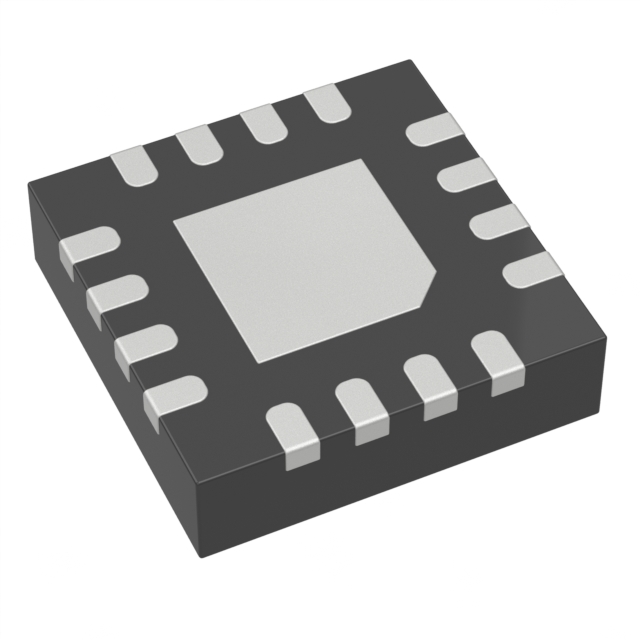
THS4509RGTT
OP Amps, Buffer Amps ICs

Not available to buy online? Want the lower wholesale price? Please Send RFQ to get best price, we will respond immediately


.png?x-oss-process=image/format,webp/resize,p_30)


THS4509RGTT Description
THS4509RGTT Description
The THS4509RGTT from Texas Instruments is a high-performance, fully differential amplifier designed for precision signal conditioning in demanding applications. Operating within a 3V to 5.25V supply range, this IC delivers exceptional bandwidth (2 GHz -3dB) and a remarkable slew rate of 6600V/µs, making it ideal for high-speed analog systems. With a gain bandwidth product of 3 GHz and ultra-low input bias current (8 µA), the THS4509RGTT ensures minimal signal distortion and high fidelity. Its differential output architecture enhances noise immunity, critical for high-frequency and high-resolution designs. Packaged in a 16-VQFN (3x3 mm) form factor with tape-and-reel (TR) delivery, it suits space-constrained PCB layouts.
THS4509RGTT Features
- Ultra-Wide Bandwidth: 2 GHz -3dB bandwidth and 3 GHz gain bandwidth product for high-speed signal processing.
- Low Power Consumption: Operates at 37.7mA supply current, balancing performance and efficiency.
- High Output Drive: Delivers 96 mA/channel output current, enabling robust signal transmission.
- Low Offset Voltage: 1 mV input offset ensures precision in DC-coupled applications.
- Robust Packaging: MSL 2 (1 Year) rated and ROHS3/REACH compliant, suitable for industrial environments.
- Differential I/O: Optimized for noise rejection in RF, medical imaging, and test equipment.
THS4509RGTT Applications
- Communications: Baseband amplification in 5G, radar, and software-defined radio (SDR) systems.
- Test & Measurement: High-speed oscilloscopes, arbitrary waveform generators, and data acquisition.
- Medical Imaging: Ultrasound and MRI signal chains requiring low noise and wide dynamic range.
- Industrial Systems: Precision ADCs/DACs, active filters, and servo control loops.
Conclusion of THS4509RGTT
The THS4509RGTT stands out as a versatile differential amplifier, combining high speed, low distortion, and robust performance in a compact package. Its superior bandwidth and slew rate make it indispensable for applications demanding fast signal fidelity and noise resilience. Whether in RF front-ends, medical diagnostics, or high-speed data converters, this amplifier delivers reliable, high-performance operation while adhering to stringent environmental and regulatory standards.
Tech Specifications
THS4509RGTT Documents
Download datasheets and manufacturer documentation for THS4509RGTT
THS4509 THS4509 Mult Dev Material Chg 29/Mar/2018 Related Parts


Shopping Guide


.png?x-oss-process=image/format,webp/resize,h_32)


©2025 ERSA Electronics Corporation.