
Texas Instruments
TL062BCD
OP Amps, Buffer Amps ICs


.png?x-oss-process=image/format,webp/resize,p_30)


TL062BCD Description
TL062BCD Description
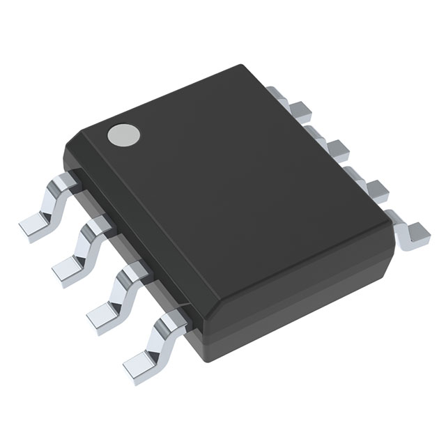
The TL062BCD from Texas Instruments is a low-power JFET-input operational amplifier housed in an 8-SOIC package, featuring dual-circuit (2-channel) architecture. Designed for precision analog applications, it operates over a wide supply voltage range of 10V to 30V with a low supply current of 200µA per channel, making it ideal for battery-powered and energy-efficient systems. The device offers high input impedance (30 pA input bias current) and low input offset voltage (2 mV), ensuring accurate signal amplification. Its 1 MHz gain bandwidth product (GBW) and 3.5V/µs slew rate provide stable performance in moderate-speed applications. The TL062BCD is RoHS3 compliant and REACH unaffected, meeting stringent environmental standards.
TL062BCD Features
- Low Power Consumption: 200µA/channel supply current extends battery life.
- JFET Input: High input impedance (30 pA bias current) minimizes loading effects.
- Wide Supply Range: 10V to 30V operation for versatile power supply compatibility.
- Moderate Speed: 1 MHz GBW and 3.5V/µs slew rate suit filtering and signal conditioning.
- Dual-Channel Design: Two independent op-amps in a compact 8-SOIC package.
- Robust Packaging: Tube packaging ensures safe handling and storage (MSL 1).
- Environmental Compliance: RoHS3 and REACH compliant for global use.
TL062BCD Applications
- Active Filters & Signal Conditioning: Ideal for low-noise, high-impedance sensor interfaces.
- Battery-Powered Systems: Portable devices, medical instruments, and IoT sensors benefit from its low power draw.
- Audio Preamplifiers: JFET input ensures minimal distortion in audio signal chains.
- Industrial Control Systems: Reliable performance in 0°C to 70°C environments.
- Test & Measurement Equipment: Precision amplification for accurate signal processing.
Conclusion of TL062BCD
The TL062BCD stands out for its low-power operation, high input impedance, and robust performance in moderate-speed analog circuits. Its dual-channel design and wide voltage range make it a versatile choice for portable, industrial, and precision applications. While classified as Last Time Buy, it remains a reliable solution for legacy designs requiring JFET op-amps with balanced performance and efficiency. Engineers seeking a cost-effective, low-noise amplifier for filtering, buffering, or signal conditioning will find the TL062BCD a compelling option.
Tech Specifications
TL062BCD Documents
Download datasheets and manufacturer documentation for TL062BCD
 TL06x(A)(B)
  EOL 22/May/2023
  TL06x(A)(B)
  Design 25/Feb/2022
 Shopping Guide


.png?x-oss-process=image/format,webp/resize,h_32)


