
Texas Instruments
TL082ACDG4
OP Amps, Buffer Amps ICs


.png?x-oss-process=image/format,webp/resize,p_30)


TL082ACDG4 Description
TL082ACDG4 Description
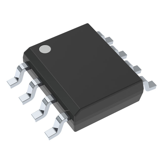
The TL082ACDG4 is a dual JFET operational amplifier from Texas Instruments, designed for high-performance analog signal processing applications. This obsolete yet highly regarded IC features a maximum supply voltage span of 30 V and a gain bandwidth product of 3 MHz, making it suitable for a wide range of precision and high-speed applications. The TL082ACDG4 operates within a temperature range of 0°C to 70°C, ensuring reliable performance in various environmental conditions. It is housed in an 8-pin SOIC package, which is ideal for surface mount applications, providing a compact and efficient solution for modern electronic designs.
TL082ACDG4 Features
- High Gain Bandwidth Product: The TL082ACDG4 boasts a gain bandwidth product of 3 MHz, enabling it to handle high-frequency signals with minimal distortion and excellent linearity.
- Low Input Bias Current: With an input bias current of just 30 pA, this op-amp minimizes the loading effect on the input signal source, making it ideal for high-impedance applications.
- High Slew Rate: A slew rate of 13 V/µs ensures that the TL082ACDG4 can handle fast-changing signals without significant phase lag or distortion.
- Wide Supply Voltage Range: The device operates with a supply voltage range of 10 V to 30 V, providing flexibility in power supply design and compatibility with various power sources.
- Low Input Offset Voltage: An input offset voltage of 3 mV ensures accurate signal processing and minimal error in precision applications.
- Dual Channel Design: The TL082ACDG4 features two independent operational amplifier channels, each capable of sourcing or sinking up to 10 mA of current, making it suitable for multi-channel signal processing tasks.
- Compliance and Packaging: The TL082ACDG4 is ROHS3 compliant and REACH unaffected, ensuring it meets stringent environmental standards. It is packaged in a tube, which is ideal for bulk handling and storage.
TL082ACDG4 Applications
The TL082ACDG4 is well-suited for a variety of applications, including:
- Audio Signal Processing: Its low input bias current and high slew rate make it ideal for high-fidelity audio amplifiers and preamplifiers, ensuring clear and distortion-free sound reproduction.
- Precision Instrumentation: The low input offset voltage and high gain bandwidth product are beneficial for precision measurement equipment, such as oscilloscopes and signal analyzers.
- Analog Signal Conditioning: The TL082ACDG4 can be used in various analog signal conditioning circuits, including filters, amplifiers, and voltage followers, to process and manipulate analog signals accurately.
- Medical Equipment: Its high performance and reliability make it suitable for medical devices that require precise signal processing, such as ECG machines and patient monitors.
Conclusion of TL082ACDG4
The TL082ACDG4 is a versatile and high-performance dual JFET operational amplifier that offers a combination of excellent technical specifications and robust performance. Despite its obsolete status, it remains a reliable choice for applications requiring high precision and high-speed signal processing. Its low input bias current, high slew rate, and wide supply voltage range make it stand out from similar models. The TL082ACDG4 is particularly well-suited for audio processing, precision instrumentation, and medical equipment, where its performance benefits can significantly enhance the accuracy and reliability of the final product.
Tech Specifications
TL082ACDG4 Documents
Download datasheets and manufacturer documentation for TL082ACDG4
 TL081(A,B,H), TL084(A,B,H)
  LF353x/TL07x/TL08x obs 26/Jul/2022
  TL081(A,B,H), TL084(A,B,H)
 Shopping Guide


.png?x-oss-process=image/format,webp/resize,h_32)


