
Texas Instruments
TL331KDBVRG4
Linear Comparators


.png?x-oss-process=image/format,webp/resize,p_30)


TL331KDBVRG4 Description
TL331KDBVRG4 Description
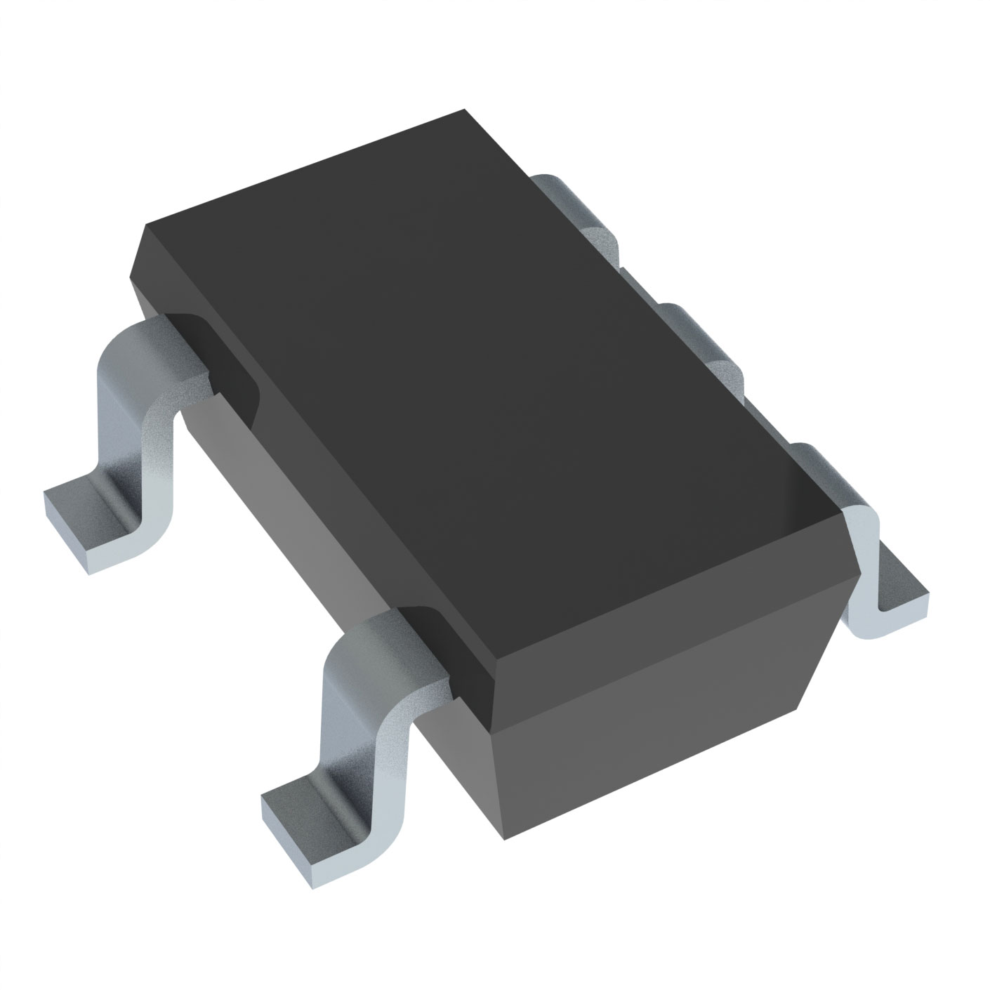
The TL331KDBVRG4 is a general-purpose comparator from Texas Instruments, designed for a wide range of applications requiring precise voltage comparison. This device is housed in a compact SOT23-5 package, making it suitable for surface-mount applications where space is a critical factor. Despite its small form factor, the TL331KDBVRG4 offers robust performance characteristics, including a typical output current of 20mA and a maximum quiescent current of 700µA. It operates over a wide supply voltage range of 2V to 36V for single supply and ±1V to ±18V for dual supply configurations. The TL331KDBVRG4 also features a maximum input offset voltage of 5mV at 30V and a maximum input bias current of 0.25µA at 5V, ensuring high accuracy and reliability in voltage comparison tasks.
TL331KDBVRG4 Features
- Wide Operating Voltage Range: The TL331KDBVRG4 can operate from 2V to 36V for single supply and ±1V to ±18V for dual supply, making it versatile for various power supply requirements.
- Low Quiescent Current: With a maximum quiescent current of 700µA, this comparator is energy-efficient, ideal for battery-powered and low-power applications.
- High Output Current: The typical output current of 20mA allows the TL331KDBVRG4 to drive loads effectively without additional amplification stages.
- Low Input Offset Voltage: A maximum input offset voltage of 5mV at 30V ensures high accuracy in voltage comparison, crucial for precision applications.
- Low Input Bias Current: The maximum input bias current of 0.25µA at 5V minimizes the impact of input loading on the circuit, enhancing overall performance.
- Compact SOT23-5 Package: The small form factor is suitable for surface-mount applications, saving valuable board space.
- Moisture Sensitivity Level 1: The TL331KDBVRG4 is rated for unlimited exposure to moisture, making it suitable for a wide range of environmental conditions.
- Compliance: The device is REACH unaffected and ROHS3 compliant, ensuring it meets environmental and regulatory standards.
TL331KDBVRG4 Applications
The TL331KDBVRG4 is ideal for applications requiring precise voltage comparison and control. Its wide operating voltage range and low quiescent current make it suitable for both low-power and high-voltage applications. Some specific use cases include:
- Battery Management Systems: The TL331KDBVRG4 can be used to monitor battery voltage levels, ensuring optimal charging and discharging cycles.
- Power Supply Monitoring: It can detect overvoltage or undervoltage conditions in power supplies, providing protection for sensitive electronic components.
- Signal Processing: The comparator can be used in signal conditioning circuits to detect specific voltage levels or transitions.
- Automotive Electronics: The device's robustness and wide operating range make it suitable for automotive applications, such as monitoring sensor signals and controlling actuators.
- Industrial Control Systems: The TL331KDBVRG4 can be used in various industrial control applications, including motor control and process monitoring.
Conclusion of TL331KDBVRG4
The TL331KDBVRG4 from Texas Instruments is a versatile and reliable comparator designed for a wide range of applications. Its wide operating voltage range, low quiescent current, and high output current make it suitable for both low-power and high-voltage applications. The device's compact SOT23-5 package and compliance with environmental and regulatory standards further enhance its appeal. While the TL331KDBVRG4 is now obsolete, its technical specifications and performance benefits make it a valuable component for engineers and designers working on legacy systems or seeking a reliable comparator for specific applications.
Tech Specifications
TL331KDBVRG4 Documents
Download datasheets and manufacturer documentation for TL331KDBVRG4
 Additional Assembly sites 21/Sep/2021
  TL331B,TL391B,TL331 Datasheet
  EOL 22/Jun/2023
  TL331B,TL391B,TL331 Datasheet
  TL331/TL331B/TL391B 11/Jun/2020
 Shopping Guide


.png?x-oss-process=image/format,webp/resize,h_32)


