

Texas Instruments
TL972QPWRQ1
OP Amps, Buffer Amps ICs

Not available to buy online? Want the lower wholesale price? Please Send RFQ to get best price, we will respond immediately


- 1+
- $0.85284
- $0.85
- 10+
- $0.75348
- $7.53
- 30+
- $0.59318
- $17.8
- 100+
- $0.53058
- $53.06
- 500+
- $0.50525
- $252.63
- 1000+
- $0.49183
- $491.83

.png?x-oss-process=image/format,webp/resize,p_30)


TL972QPWRQ1 Description
TL972QPWRQ1 Description
The TL972QPWRQ1 is a high-performance, dual operational amplifier (op-amp) designed and manufactured by Texas Instruments. It is part of the OP Amps, Buffer Amps ICs category and is specifically tailored for automotive applications. This IC features a wide voltage supply span, ranging from 2.7 V to 12 V, and is REACH unaffected, ensuring compliance with environmental regulations. The TL972QPWRQ1 is also RoHS3 compliant, making it suitable for use in electronic devices that adhere to the Restriction of Hazardous Substances directive.
TL972QPWRQ1 Features
- Voltage Supply Span: The TL972QPWRQ1 operates over a wide voltage range, from 2.7 V to 12 V, providing flexibility in various power supply scenarios.
- Gain Bandwidth Product: With a gain bandwidth product of 12 MHz, this op-amp offers excellent high-frequency performance.
- Slew Rate: The device boasts a fast slew rate of 5V/µs, ensuring quick response times in signal processing.
- Input Bias Current: The low input bias current of 200 nA contributes to high input impedance and minimal loading effects on the source.
- Input Offset Voltage: The TL972QPWRQ1 has a low input offset voltage of 1 mV, enhancing accuracy in signal amplification.
- Supply Current: The device consumes a low supply current of 2mA for both channels, making it energy-efficient.
- Output Current: Each channel can deliver up to 80 mA, providing ample drive capability for various loads.
- Mounting Type: The TL972QPWRQ1 is surface-mountable, facilitating integration into compact electronic designs.
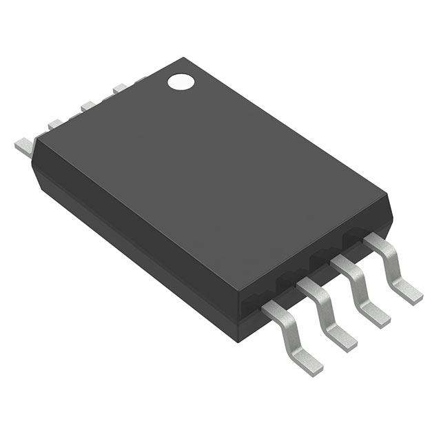
- Package: It is available in an 8-pin TSSOP package, which is suitable for high-density PCB layouts.
TL972QPWRQ1 Applications
The TL972QPWRQ1 is ideal for a variety of applications where high performance, reliability, and compliance with environmental standards are critical. Some specific use cases include:
- Automotive Sensor Interfaces: Due to its automotive grade and wide supply voltage range, it is well-suited for interfacing with various sensors in automotive systems.
- Industrial Control Systems: The high slew rate and low input bias current make it suitable for use in precision control systems.
- Audio Amplification: The combination of low noise and high slew rate makes it an excellent choice for audio applications requiring clear and dynamic sound reproduction.
Conclusion of TL972QPWRQ1
The TL972QPWRQ1 is a versatile and high-performance dual op-amp that stands out in the market due to its automotive grade, wide voltage supply span, and compliance with environmental regulations. Its unique combination of technical specifications makes it an excellent choice for applications requiring high accuracy, fast response times, and robust performance in challenging environments. With its low power consumption and ability to handle high output currents, the TL972QPWRQ1 is a reliable component for a wide range of electronic systems.
Tech Specifications
TL972QPWRQ1 Documents
Download datasheets and manufacturer documentation for TL972QPWRQ1
Mechanical Outline Drawing Product Change Notification_2024_12_18 (PDF) Product Change Notification (PDF) TL972QPWRQ1 Symbol & Footprint by SnapMagic TL972 TINA-TI Reference Design TL972 PSpice Model TL972 TINA-TI Spice Model Related Parts


Shopping Guide


.png?x-oss-process=image/format,webp/resize,h_32)


©2025 ERSA Electronics Corporation.