
Texas Instruments
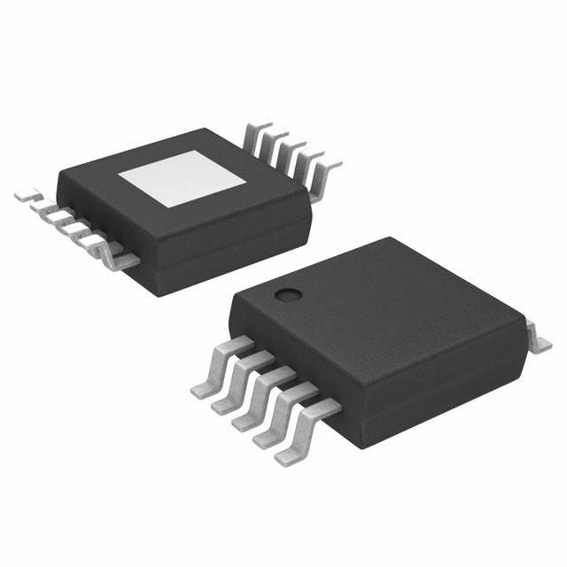
TLC073CDGQ
OP Amps, Buffer Amps ICs


.png?x-oss-process=image/format,webp/resize,p_30)


TLC073CDGQ Description
TLC073CDGQ Description
The TLC073CDGQ is a high-performance CMOS operational amplifier designed for automotive applications, manufactured by Texas Instruments. This dual-channel amplifier features a wide supply voltage range from 4.5 V to 16 V, making it suitable for a variety of power supply configurations. With a gain bandwidth product of 10 MHz and a slew rate of 19 V/µs, the TLC073CDGQ delivers excellent performance in high-speed signal processing applications. The device operates within a temperature range of 0°C to 70°C (TA), ensuring reliable performance in automotive environments.
TLC073CDGQ Features
- Wide Supply Voltage Range: The TLC073CDGQ supports a supply voltage span from 4.5 V to 16 V, providing flexibility in various power supply designs.
- High Gain Bandwidth Product: With a gain bandwidth product of 10 MHz, this amplifier ensures high-frequency performance, making it ideal for applications requiring fast signal processing.
- Low Input Bias Current: The input bias current is as low as 1.5 pA, minimizing the impact of input current on the signal source.
- High Slew Rate: A slew rate of 19 V/µs allows for rapid response to input signal changes, reducing distortion in high-frequency applications.
- Low Input Offset Voltage: The input offset voltage is only 390 µV, ensuring accurate signal amplification and minimizing errors.
- Automotive Grade: The TLC073CDGQ is designed to meet the stringent requirements of automotive applications, ensuring reliability and durability.
- Compliance and Safety: The device is REACH unaffected and RoHS3 compliant, adhering to environmental and safety standards.
- Moisture Sensitivity Level: With an MSL of 1 (Unlimited), the TLC073CDGQ is suitable for surface mount applications without the need for special handling precautions.
TLC073CDGQ Applications
The TLC073CDGQ is well-suited for a range of automotive applications where high performance and reliability are critical. Specific use cases include:
- Automotive Signal Processing: Ideal for amplifying and conditioning signals in automotive electronic control units (ECUs) and sensor interfaces.
- High-Speed Data Acquisition: Suitable for applications requiring fast and accurate signal processing, such as automotive diagnostic systems.
- Power Management: The wide supply voltage range and low power consumption make it suitable for power management circuits in automotive systems.
- Audio Systems: Provides high-quality signal amplification for automotive audio systems, ensuring clear and distortion-free sound.
Conclusion of TLC073CDGQ
The TLC073CDGQ from Texas Instruments is a robust and versatile CMOS operational amplifier designed to meet the demanding requirements of automotive applications. Its wide supply voltage range, high gain bandwidth product, and low input bias current make it an excellent choice for high-speed signal processing and power management tasks. The device's automotive grade construction, compliance with environmental and safety standards, and low moisture sensitivity level further enhance its suitability for surface mount applications in automotive environments. Whether used in signal processing, data acquisition, or power management, the TLC073CDGQ delivers reliable performance and exceptional value.
Tech Specifications
TLC073CDGQ Documents
Download datasheets and manufacturer documentation for TLC073CDGQ
 Assembly/Wafer Fab Site 31/Jul/2023
  TLC070-75, TLC07xA
  TLC070-75, TLC07xA
  SOT23, VSSOP Cu Wire 28/Jun/2013 Copper Wire Revision C 24/Sep/2014
 Shopping Guide


.png?x-oss-process=image/format,webp/resize,h_32)


