

Texas Instruments
TLC2272ACPW
OP Amps, Buffer Amps ICs

Not available to buy online? Want the lower wholesale price? Please Send RFQ to get best price, we will respond immediately


.png?x-oss-process=image/format,webp/resize,p_30)


TLC2272ACPW Description
TLC2272ACPW Description
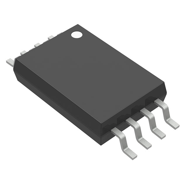
The TLC2272ACPW is a CMOS operational amplifier from Texas Instruments, featuring a dual-channel design in an 8-pin TSSOP package. This IC is designed for a wide range of linear amplifier applications, offering a robust set of performance characteristics. The TLC2272ACPW operates within a supply voltage range of 4.4V to 16V, making it suitable for both low and high voltage applications. It boasts a gain bandwidth product of 2.25 MHz and a slew rate of 3.6V/µs, ensuring high-speed signal processing capabilities. The device is optimized for low input bias current, with a value of only 1 pA, which is ideal for precision applications. Additionally, it features a low input offset voltage of 300 µV, contributing to its accuracy and reliability.
TLC2272ACPW Features
- High Gain Bandwidth Product: With a gain bandwidth product of 2.25 MHz, the TLC2272ACPW can handle high-frequency signals effectively, making it suitable for applications requiring fast response times.
- Low Input Bias Current: The extremely low input bias current of 1 pA ensures minimal loading on the signal source, which is crucial for high-impedance sensor interfaces.
- Wide Supply Voltage Range: The TLC2272ACPW operates from 4.4V to 16V, providing flexibility in power supply requirements and compatibility with various power sources.
- High Slew Rate: A slew rate of 3.6V/µs allows for rapid signal transitions, ensuring minimal distortion in high-speed applications.
- Low Input Offset Voltage: The low input offset voltage of 300 µV enhances the accuracy of the amplifier, making it suitable for precision measurement applications.
- Dual Channel Design: The TLC2272ACPW features two independent amplifier channels, allowing for multiple signal processing paths within a single package.
- Surface Mount Package: The 8-pin TSSOP package is ideal for surface mount applications, providing a compact and reliable solution for modern PCB designs.
- Compliance and Reliability: The TLC2272ACPW is REACH unaffected and RoHS3 compliant, ensuring environmental and regulatory compliance. It also has a moisture sensitivity level of 1 (unlimited), making it suitable for a wide range of manufacturing environments.
TLC2272ACPW Applications
The TLC2272ACPW is well-suited for a variety of applications due to its versatile performance characteristics. Some specific use cases include:
- Signal Conditioning: Ideal for conditioning signals from high-impedance sensors, such as photodiodes and piezoelectric sensors, due to its low input bias current.
- High-Speed Filtering: The high gain bandwidth product and slew rate make it suitable for active filters in-speed high signal processing applications.
- Precision Measurement: The low input offset voltage and high accuracy make it ideal for precision instrumentation and measurement devices.
- Audio Applications: The TLC2272ACPW can be used in audio signal processing due to its ability to handle high-frequency signals with minimal distortion.
- Industrial Control Systems: The wide supply voltage range and robust performance make it suitable for industrial control systems where reliability and accuracy are critical.
Conclusion of TLC2272ACPW
The TLC2272ACPW from Texas Instruments is a versatile CMOS operational amplifier that offers a combination of high performance and reliability. Its dual-channel design, wide supply voltage range, and low input bias current make it suitable for a wide range of applications, from precision measurement to high-speed signal processing. Despite being marked as obsolete, the TLC2272ACPW remains a valuable component for engineers and designers looking for a reliable and high-performance solution in their projects.
Tech Specifications
TLC2272ACPW Documents
Download datasheets and manufacturer documentation for TLC2272ACPW
TLC2272ACPW Update 10/Mar/2023 TLC2272x(A) Datasheet Mult Dev EOL 7/Sep/2023 Design 22/Feb/2022 Related Parts


Shopping Guide


.png?x-oss-process=image/format,webp/resize,h_32)


©2025 ERSA Electronics Corporation.