
 German
 Japanese
 Portuguese
 Korea
Korea
 Mexico
 Dutch
Dutch


Texas Instruments
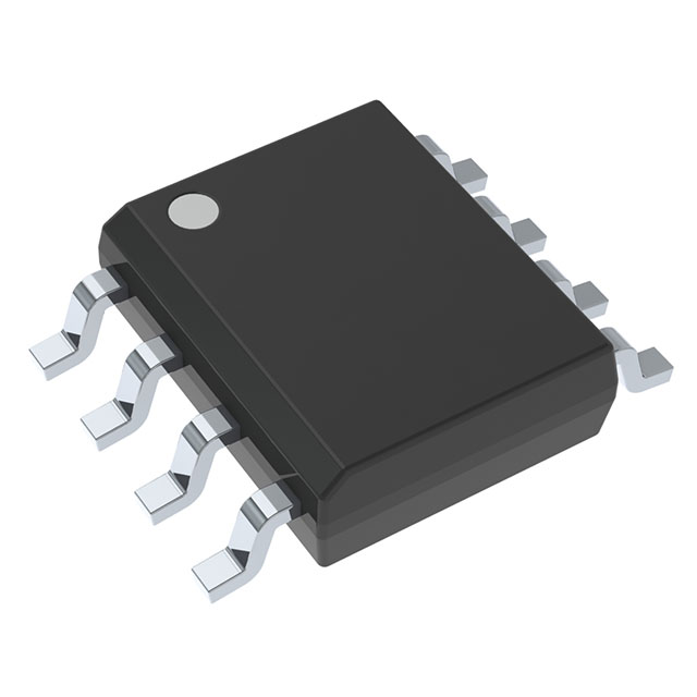
TLC25L2BCD

Why Choose Us?
Professional Platform
B2B & B2C purchasingDelivery at full speed
1-2 days deliveryWide variety
Original manufacturers365 days guarantee
Responsible quality
.png)


Tech Specifications
TLC25L2BCD Description
TLC25L2BCD Description
The TLC25L2BCD is a high-performance CMOS operational amplifier from Texas Instruments, designed for a wide range of linear applications. This device features a dual-circuit configuration, housed in an 8-pin SOIC package, making it suitable for surface-mount applications. The TLC25L2BCD operates within a supply voltage range of 1.4 V to 16 V, providing flexibility for various power supply requirements. It is capable of operating within an ambient temperature range of 0°C to 70°C, making it ideal for general industrial and commercial applications.
TLC25L2BCD Features
- Wide Supply Voltage Range: The TLC25L2BCD can operate from a supply voltage as low as 1.4 V up to 16 V, offering significant flexibility in power supply design.
- Low Power Consumption: With a supply current of only 29 µA per channel, this device is highly energy-efficient, making it suitable for battery-powered and low-power applications.
- High Slew Rate: The 2.9 V/µs slew rate ensures fast response times, making it ideal for high-frequency signal processing.
- High Gain Bandwidth Product: The 110 kHz gain bandwidth product provides excellent performance in signal amplification and filtering applications.
- Low Input Bias Current: The extremely low input bias current of 0.7 pA minimizes the impact of input currents on the signal, ensuring high accuracy in precision applications.
- Low Input Offset Voltage: The 235 µV input offset voltage contributes to high accuracy in signal conditioning and measurement applications.
- Surface Mount Compatibility: The surface-mount package type facilitates easy integration into modern PCB designs.
- Compliance and Safety: The TLC25L2BCD is REACH unaffected and RoHS3 compliant, ensuring it meets environmental and safety standards.
TLC25L2BCD Applications
The TLC25L2BCD is well-suited for a variety of applications due to its versatile performance characteristics. Some specific use cases include:
- Signal Conditioning: Ideal for amplifying and conditioning low-level signals in sensors and transducers.
- Analog Filters: The high gain bandwidth product and low input offset voltage make it suitable for designing precision analog filters.
- Battery-Powered Devices: The low power consumption and wide supply voltage range make it a great choice for portable and battery-operated equipment.
- Industrial Control Systems: The wide operating temperature range and robust performance make it suitable for use in industrial control and automation systems.
- Medical Equipment: The low input bias current and high accuracy are beneficial for medical devices requiring precise signal processing.
Conclusion of TLC25L2BCD
The TLC25L2BCD from Texas Instruments is a versatile and high-performance CMOS operational amplifier that offers a wide range of benefits for various applications. Its wide supply voltage range, low power consumption, and high slew rate make it an excellent choice for both low-power and high-frequency applications. The low input bias current and low input offset voltage ensure high accuracy and precision, making it suitable for demanding signal processing tasks. While the product is now obsolete, its legacy continues to influence the design of modern operational amplifiers. For those seeking a reliable and efficient solution for their analog signal processing needs, the TLC25L2BCD remains a notable option.
FAQ
Not available to buy online? Want the lower wholesale price? Please Send RFQ to get best price, we will respond immediately


.png?x-oss-process=image/format,webp/resize,h_32)


