
Texas Instruments
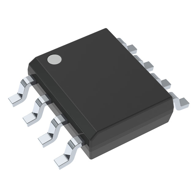
TLC4502ACDR
OP Amps, Buffer Amps ICs


.png?x-oss-process=image/format,webp/resize,p_30)


TLC4502ACDR Description
TLC4502ACDR Description
The TLC4502ACDR is a high-performance, dual-channel CMOS operational amplifier (op-amp) from Texas Instruments. It is designed for applications requiring low power, low noise, and high bandwidth. The device operates over a wide supply voltage range of 4 V to 6 V, making it suitable for various power supply configurations. The TLC4502ACDR is RoHS compliant and REACH unaffected, ensuring environmental compliance in electronic designs.
TLC4502ACDR Features
- Voltage - Supply Span (Max): 6 V, Voltage - Supply Span (Min): 4 V
- Gain Bandwidth Product: 4.7 MHz, providing high-speed amplification
- Slew Rate: 2.5 V/µs, ensuring fast response times
- Current - Input Bias: 1 pA, minimizing input current consumption
- Current - Supply: 2.5 mA (x2 Channels), suitable for low-power applications
- Current - Output / Channel: 50 mA, providing sufficient drive capability
- Voltage - Input Offset: 10 µV, ensuring high accuracy
- Operating Temperature: 0°C ~ 70°C, suitable for a wide range of environments
- Moisture Sensitivity Level (MSL): 1 (Unlimited), allowing for flexible handling and storage
- Mounting Type: Surface Mount, facilitating integration into PCB designs
- Number of Circuits: 2, providing dual-channel functionality in a single package
- Package: Tape & Reel (TR), suitable for automated assembly processes
TLC4502ACDR Applications
The TLC4502ACDR is ideal for applications where low power, low noise, and high bandwidth are required. Some specific use cases include:
- Audio Amplification: The low noise and high bandwidth make it suitable for audio signal amplification in consumer electronics.
- Sensor Signal Conditioning: The low input bias current and high input offset voltage make it ideal for conditioning signals from sensors in industrial and automotive applications.
- Data Acquisition Systems: The high slew rate and bandwidth are beneficial for processing signals in data acquisition systems.
- Portable Electronics: The low power consumption and wide operating temperature range make it suitable for portable electronic devices.
Conclusion of TLC4502ACDR
The TLC4502ACDR is a versatile, dual-channel CMOS op-amp that offers a combination of low power, low noise, and high bandwidth. Its wide supply voltage range, RoHS compliance, and REACH unaffected status make it an excellent choice for a variety of applications in the electronics industry. With its unique features and advantages, the TLC4502ACDR stands out as a reliable and efficient solution for demanding applications.
Tech Specifications
TLC4502ACDR Documents
Download datasheets and manufacturer documentation for TLC4502ACDR
 TLC4501/A, TLC4502/A
 Shopping Guide


.png?x-oss-process=image/format,webp/resize,h_32)


