

Texas Instruments
TLC4502MDG4
OP Amps, Buffer Amps ICs

Not available to buy online? Want the lower wholesale price? Please Send RFQ to get best price, we will respond immediately


.png?x-oss-process=image/format,webp/resize,p_30)


TLC4502MDG4 Description
TLC4502MDG4 Description
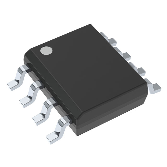
The TLC4502MDG4 is a CMOS operational amplifier from Texas Instruments, featuring a dual-circuit configuration in an 8SOIC package. This IC is designed to offer high performance in a compact form factor, making it suitable for a wide range of linear amplifier applications. Despite being marked as obsolete, the TLC4502MDG4 remains a reliable choice for engineers and designers looking for specific operational amplifier characteristics.
TLC4502MDG4 Features
- Supply Voltage Span: The TLC4502MDG4 operates within a supply voltage range of 4 V to 6 V, providing flexibility in power supply design.
- Gain Bandwidth Product: With a gain bandwidth product of 4.7 MHz, this amplifier ensures high-frequency performance suitable for various signal processing tasks.
- Slew Rate: A slew rate of 2.5 V/µs allows for rapid response to input signal changes, minimizing distortion in high-frequency applications.
- Low Input Bias Current: The extremely low input bias current of 1 pA makes the TLC4502MDG4 ideal for applications requiring high input impedance, such as precision instrumentation.
- Supply Current: The total supply current for both channels is 2.5 mA, contributing to energy-efficient designs.
- Output Current: Each channel can deliver up to 50 mA of output current, supporting robust load driving capabilities.
- Input Offset Voltage: The low input offset voltage of 10 µV ensures high accuracy in signal amplification.
- Compliance and Packaging: The TLC4502MDG4 is RoHS3 compliant and REACH unaffected, meeting environmental and regulatory standards. It is packaged in bulk, suitable for surface mount applications and has a moisture sensitivity level (MSL) of 1, indicating it is safe for unlimited exposure to ambient conditions.
TLC4502MDG4 Applications
The TLC4502MDG4 is well-suited for applications that demand high precision and low power consumption. Its dual-channel design and CMOS technology make it ideal for:
- Precision Signal Amplification: In instrumentation and measurement systems where accuracy and low noise are critical.
- Analog Signal Processing: For filtering, conditioning, and amplifying analog signals in communication and control systems.
- Battery-Powered Devices: Due to its low supply current, the TLC4502MDG4 is suitable for portable and battery-operated equipment.
- Medical Equipment: Its low input bias current and high input impedance make it a good fit for medical devices requiring high precision and low noise.
Conclusion of TLC4502MDG4
The TLC4502MDG4, despite being obsolete, continues to offer significant advantages in specific applications. Its combination of low power consumption, high precision, and robust output capabilities make it a reliable choice for engineers who require a dual-channel CMOS operational amplifier. While newer alternatives may exist, the TLC4502MDG4 remains a viable option for those who need its unique set of features and performance characteristics.
Tech Specifications
TLC4502MDG4 Documents
Download datasheets and manufacturer documentation for TLC4502MDG4
Mult Dev 30/Oct/2019 TLC4501/A, TLC4502/A DK OBS NOTICE Related Parts


Shopping Guide


.png?x-oss-process=image/format,webp/resize,h_32)


©2025 ERSA Electronics Corporation.