
 German
 Japanese
 Portuguese
 Korea
Korea
 Mexico
 Dutch
Dutch


Texas Instruments
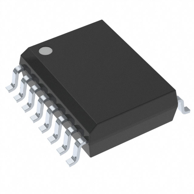
TLE2024BMDWG4

Why Choose Us?
Professional Platform
B2B & B2C purchasingDelivery at full speed
1-2 days deliveryWide variety
Original manufacturers365 days guarantee
Responsible quality
.png)


Tech Specifications
TLE2024BMDWG4 Description
TLE2024BMDWG4 Description
The TLE2024BMDWG4 is a general-purpose operational amplifier (op-amp) from Texas Instruments, designed for a wide range of applications requiring high performance and reliability. This quad-channel op-amp is part of the Excalibur™ series, known for its robustness and versatility. It features a wide supply voltage range, from 4 V to 40 V, making it suitable for various power supply configurations. The TLE2024BMDWG4 offers a gain bandwidth product of 2.8 MHz, ensuring high-frequency performance and stability. Its low input bias current of 35 nA and input offset voltage of 500 µV contribute to its precision and accuracy in signal processing. The device is housed in a surface-mount package, specifically a tube, which facilitates easy integration into compact designs. Despite its obsolescence status, the TLE2024BMDWG4 remains a reliable choice for engineers seeking a proven solution in the linear IC chips category.
TLE2024BMDWG4 Features
- Wide Supply Voltage Range: Operates from 4 V to 40 V, providing flexibility in power supply requirements.
- High Gain Bandwidth Product: 2.8 MHz ensures stable performance across a broad frequency spectrum.
- Low Input Bias Current: 35 nA minimizes the impact on sensitive input signals, enhancing precision.
- Low Input Offset Voltage: 500 µV ensures accurate signal processing and minimal error.
- Quad-Channel Configuration: Four independent op-amps in a single package, ideal for multi-channel applications.
- High Slew Rate: 0.7 V/µs for fast response times and minimal signal distortion.
- Surface-Mount Package: Tube packaging for easy integration into compact and robust designs.
- Compliance and Reliability: REACH unaffected and RoHS3 compliant, ensuring environmental and regulatory standards are met.
- Moisture Sensitivity Level: MSL 1 (Unlimited), suitable for a wide range of environmental conditions.
TLE2024BMDWG4 Applications
The TLE2024BMDWG4 is well-suited for a variety of applications where precision, reliability, and versatility are paramount. Its wide supply voltage range and high gain bandwidth product make it ideal for:
- Signal Conditioning: Amplifying and processing analog signals in industrial control systems.
- Filter Design: Implementing active filters for noise reduction and signal shaping.
- Sensor Interfaces: Amplifying weak signals from sensors in automotive and industrial applications.
- Power Management: Managing power distribution and regulation in electronic systems.
- Medical Equipment: Ensuring accurate signal processing in medical monitoring devices.
- Consumer Electronics: Enhancing audio and video signal quality in consumer devices.
Conclusion of TLE2024BMDWG4
The TLE2024BMDWG4 is a versatile and reliable general-purpose op-amp that offers a wide range of technical specifications and performance benefits. Its wide supply voltage range, high gain bandwidth product, and low input bias current make it suitable for a variety of applications, from signal conditioning to power management. Despite its obsolescence status, the TLE2024BMDWG4 remains a robust choice for engineers seeking a proven solution in the linear IC chips category. Its compliance with environmental and regulatory standards further enhances its appeal in the electronics industry.
FAQ
Not available to buy online? Want the lower wholesale price? Please Send RFQ to get best price, we will respond immediately


.png?x-oss-process=image/format,webp/resize,h_32)


