
Texas Instruments
TLE2071ACD
OP Amps, Buffer Amps ICs


.png?x-oss-process=image/format,webp/resize,p_30)


TLE2071ACD Description
TLE2071ACD Description
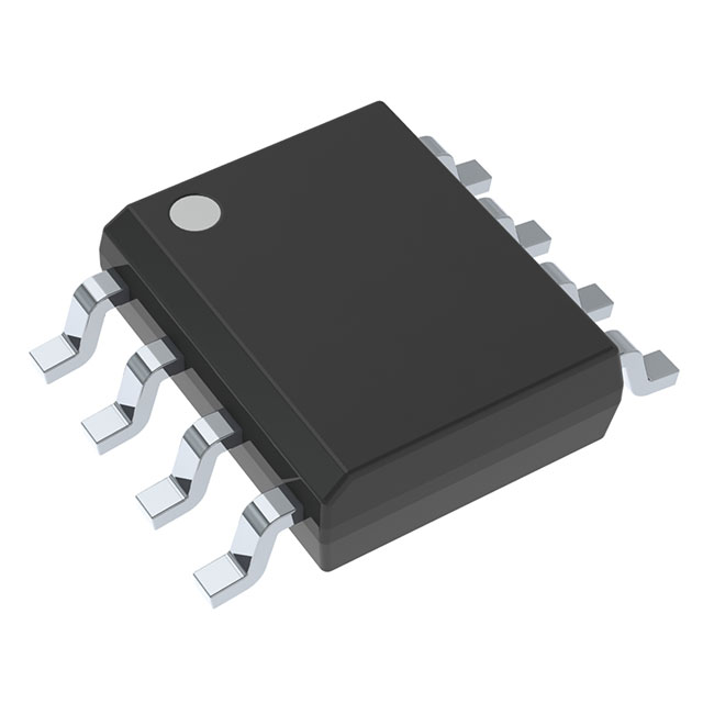
The TLE2071ACD from Texas Instruments is a high-performance JFET-input operational amplifier from the Excalibur™ series, designed for precision analog applications. Housed in an 8-SOIC package, this single-channel op-amp operates over a wide supply voltage range of 4.5V to 38V, making it versatile for industrial and instrumentation systems. With an ultra-low input bias current of 20 pA and a gain bandwidth product of 10 MHz, it ensures high accuracy and speed in signal conditioning. The 45V/µs slew rate and 48 mA output current capability further enhance its dynamic performance, while its low input offset voltage (470 µV) minimizes errors in DC-sensitive circuits.
TLE2071ACD Features
- Low Power Consumption: Only 1.7mA supply current for energy-efficient designs.
- Wide Supply Range: Supports 4.5V to 38V, ideal for battery-powered and high-voltage systems.
- High-Speed Performance: 10 MHz GBW and 45V/µs slew rate for fast signal processing.
- JFET Input: 20 pA input bias current ensures minimal loading in high-impedance circuits.
- Robust Output: 48 mA output drive for driving capacitive or resistive loads.
- Reliable Packaging: MSL 1 (Unlimited) moisture sensitivity ensures long-term storage stability.
- Compliance: ROHS3 and REACH unaffected, meeting environmental standards.
TLE2071ACD Applications
- Precision Instrumentation: Ideal for data acquisition systems and sensor interfaces due to low noise and high accuracy.
- Active Filters: High bandwidth and slew rate make it suitable for audio and signal processing filters.
- Industrial Control Systems: Operates reliably in harsh environments (0°C to 70°C).
- Medical Equipment: Low input bias current benefits biomedical signal amplification.
- Test & Measurement: Used in oscilloscopes and function generators for high-fidelity signal reproduction.
Conclusion of TLE2071ACD
The TLE2071ACD stands out for its combination of speed, precision, and wide voltage operation, making it a superior choice for demanding analog designs. While it is currently in Last Time Buy status, its JFET input, high slew rate, and robust output ensure it remains a reliable solution for legacy and new systems requiring high-performance amplification. Engineers in industrial, medical, and test equipment sectors will find it particularly valuable for maintaining signal integrity in critical applications.
Tech Specifications
TLE2071ACD Documents
Download datasheets and manufacturer documentation for TLE2071ACD
 TLE207x, TLE207xA Datasheet
  EOL 22/May/2023
  TLE207x, TLE207xA Datasheet
  Mult Devices Font 21/Apr/2018 Design 25/Feb/2022
 Shopping Guide


.png?x-oss-process=image/format,webp/resize,h_32)


