

Texas Instruments
TLE2072MJGB
OP Amps, Buffer Amps ICs

Not available to buy online? Want the lower wholesale price? Please Send RFQ to get best price, we will respond immediately


.png?x-oss-process=image/format,webp/resize,p_30)


TLE2072MJGB Description
TLE2072MJGB Description
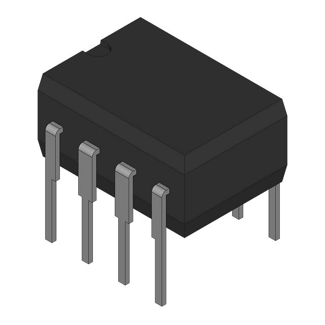
The TLE2072MJGB is a military-grade, dual-channel operational amplifier designed for high-performance applications requiring robustness and reliability. Manufactured by Texas Instruments, this amplifier is part of the Excalibur™ series, known for its exceptional performance characteristics. The TLE2072MJGB features a wide supply voltage range from 4.5 V to 38 V, making it suitable for a variety of power supply configurations. It boasts a high slew rate of 45 V/µs and a gain bandwidth product of 10 MHz, ensuring fast and precise signal processing. The amplifier is housed in a through-hole package, which is ideal for applications requiring mechanical stability and ease of installation on printed circuit boards.
TLE2072MJGB Features
- Wide Supply Voltage Range: The TLE2072MJGB operates over a supply voltage range from 4.5 V to 38 V, providing flexibility in power supply design and compatibility with various system voltages.
- High Slew Rate: With a slew rate of 45 V/µs, the TLE2072MJGB can handle high-frequency signals with minimal distortion, making it suitable for applications requiring fast transient response.
- Gain Bandwidth Product: The 10 MHz gain bandwidth product ensures high-frequency performance, enabling the amplifier to maintain signal integrity across a broad frequency spectrum.
- Low Input Bias Current: The low input bias current of 20 pA minimizes the effect of source impedance on the input signal, resulting in higher accuracy and lower noise.
- Low Input Offset Voltage: The 490 µV input offset voltage ensures high precision in signal amplification, making the TLE2072MJGB suitable for applications requiring high accuracy.
- High Output Current: Each channel can deliver up to 48 mA of output current, providing sufficient drive capability for various loads.
- Military-Grade Reliability: The TLE2072MJGB is designed to meet the stringent requirements of military-grade applications, ensuring high reliability and performance in harsh operating conditions.
- Compliance: The product is REACH unaffected and RoHS3 compliant, adhering to environmental and safety standards.
TLE2072MJGB Applications
The TLE2072MJGB is ideal for a range of applications where high performance and reliability are critical. Its wide supply voltage range and high slew rate make it suitable for:
- Military and Aerospace Systems: Ideal for radar systems, avionics, and other high-reliability applications where precision and robustness are paramount.
- Industrial Controls: Suitable for motor control, power management, and other industrial applications requiring high-frequency signal processing.
- Medical Equipment: Can be used in diagnostic equipment and monitoring systems where accuracy and reliability are crucial.
- Telecommunications: Ideal for signal processing in communication systems, ensuring high-speed data transmission with minimal distortion.
Conclusion of TLE2072MJGB
The TLE2072MJGB is a versatile and high-performance dual-channel operational amplifier designed to meet the demanding requirements of military and industrial applications. Its wide supply voltage range, high slew rate, and low input bias current make it an excellent choice for applications requiring precision and reliability. The military-grade reliability and compliance with environmental standards further enhance its suitability for critical applications. Whether used in radar systems, industrial controls, or medical equipment, the TLE2072MJGB delivers outstanding performance and robustness, making it a preferred choice for engineers and designers in the electronics industry.
Tech Specifications
TLE2072MJGB Documents
Download datasheets and manufacturer documentation for TLE2072MJGB
Related Parts


Shopping Guide


.png?x-oss-process=image/format,webp/resize,h_32)


©2025 ERSA Electronics Corporation.