
Texas Instruments
TLV1812QDRQ1
Linear Comparators


.png?x-oss-process=image/format,webp/resize,p_30)


TLV1812QDRQ1 Description
TLV1812QDRQ1 Description
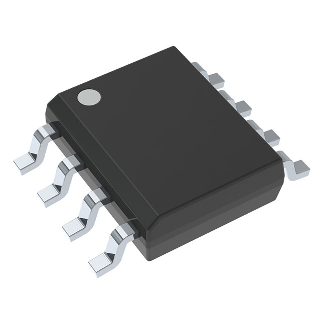
The TLV1812QDRQ1 is a high-performance, automotive-grade, dual micro-power comparator designed by Texas Instruments. This device is specifically engineered to meet the stringent requirements of automotive applications while delivering exceptional performance and reliability. With a wide supply voltage range of 2.4V to 40V, the TLV1812QDRQ1 is suitable for a variety of power supply configurations, making it highly versatile for different automotive systems.
TLV1812QDRQ1 Features
- High CMRR and PSRR: The TLV1812QDRQ1 boasts a typical Common Mode Rejection Ratio (CMRR) and Power Supply Rejection Ratio (PSRR) of 100dB, ensuring high accuracy and stability in the presence of noise and power supply variations.
- Low Quiescent Current: With a maximum quiescent current of only 9µA, this comparator is highly energy-efficient, making it ideal for applications where power consumption is a critical concern.
- High Output Current: The device can deliver a typical output current of 30mA, providing robust performance even under demanding load conditions.
- Low Input Offset Voltage: The maximum input offset voltage of 3mV at 12V ensures precise comparisons, minimizing errors in signal processing.
- Ultra-Low Input Bias Current: The maximum input bias current of 0.15pA at 12V further enhances the accuracy and reliability of the comparator, especially in high-impedance circuits.
- Fast Propagation Delay: With a typical propagation delay of 900ns, the TLV1812QDRQ1 offers quick response times, making it suitable for applications requiring rapid signal processing.
- Dual Comparator Configuration: The device includes two independent comparators, allowing for more complex signal processing and control functions within a single package.
- Surface Mount Packaging: The TLV1812QDRQ1 is available in a surface mount package (Tape & Reel), facilitating easy integration into modern automotive electronic systems.
- Moisture Sensitivity Level (MSL) 1: This indicates that the device is not moisture-sensitive, ensuring reliability and longevity in various environmental conditions.
- Compliance and Safety: The TLV1812QDRQ1 is REACH unaffected and RoHS3 compliant, adhering to the highest environmental and safety standards.
TLV1812QDRQ1 Applications
The TLV1812QDRQ1 is particularly well-suited for automotive applications due to its robustness, low power consumption, and high performance. Specific use cases include:
- Battery Management Systems: The low quiescent current and high CMRR make it ideal for monitoring and managing battery health in electric and hybrid vehicles.
- Engine Control Units (ECUs): The wide supply voltage range and high output current enable precise control and monitoring of engine parameters.
- Safety-Critical Systems: The dual comparator configuration and fast propagation delay are beneficial for applications such as airbag deployment systems, where rapid and accurate signal processing is crucial.
- Powertrain Control: The device's ability to operate over a wide voltage range and its low power consumption make it suitable for managing powertrain components.
- Sensor Interfaces: The low input offset voltage and ultra-low input bias current ensure accurate signal processing for various sensors used in automotive systems.
Conclusion of TLV1812QDRQ1
The TLV1812QDRQ1 from Texas Instruments is a standout choice for automotive applications requiring high performance, reliability, and efficiency. Its unique features, such as the high CMRR and PSRR, low quiescent current, and fast propagation delay, provide significant advantages over similar models. The dual comparator configuration and wide supply voltage range further enhance its versatility, making it suitable for a wide range of automotive systems. Whether used in battery management, engine control, or safety-critical applications, the TLV1812QDRQ1 delivers exceptional performance and reliability, ensuring it remains a preferred choice for automotive engineers and designers.
Tech Specifications
TLV1812QDRQ1 Documents
Download datasheets and manufacturer documentation for TLV1812QDRQ1
 TLV181x-Q1, TLV182x-Q1
 Shopping Guide


.png?x-oss-process=image/format,webp/resize,h_32)


