
Texas Instruments
TLV2401CDBVR
OP Amps, Buffer Amps ICs


.png?x-oss-process=image/format,webp/resize,p_30)


TLV2401CDBVR Description
TLV2401CDBVR Description
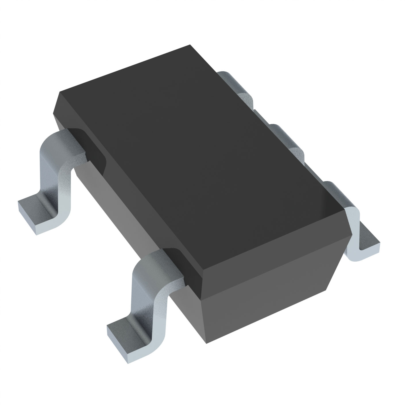
The TLV2401CDBVR is a general-purpose operational amplifier (op-amp) from Texas Instruments, designed for a wide range of applications requiring low power consumption and high performance. This op-amp is housed in a compact SOT23-5 package, making it ideal for space-constrained designs. It operates over a wide supply voltage range of 2.5 V to 16 V, ensuring flexibility in various power supply configurations. The TLV2401CDBVR features a gain bandwidth product of 5.5 kHz, a slew rate of 0.0025 V/µs, and an input bias current of just 100 pA, which minimizes the impact on sensitive input signals. With a supply current of 900 nA and an input offset voltage of 390 µV, this op-amp is optimized for low power and high precision applications.
TLV2401CDBVR Features
- Low Power Consumption: The TLV2401CDBVR consumes only 900 nA of supply current, making it highly energy-efficient and suitable for battery-operated and low-power systems.
- Wide Supply Voltage Range: With a supply voltage range of 2.5 V to 16 V, this op-amp can be used in a variety of power supply environments, from low-voltage portable devices to higher-voltage industrial applications.
- High Input Impedance: The low input bias current of 100 pA ensures minimal loading on the input signal source, preserving signal integrity.
- Precision Performance: The input offset voltage of 390 µV and the gain bandwidth product of 5.5 kHz provide high precision and stable performance in signal processing applications.
- Compact Packaging: The SOT23-5 package offers a small footprint, making it ideal for dense printed circuit board (PCB) layouts and portable electronics.
- Compliance and Reliability: The TLV2401CDBVR is REACH unaffected and ROHS3 compliant, ensuring environmental safety and regulatory compliance. It also has a moisture sensitivity level (MSL) of 1, making it suitable for unlimited storage and handling conditions.
TLV2401CDBVR Applications
The TLV2401CDBVR is well-suited for a variety of applications where low power consumption, high precision, and compact size are critical. Some specific use cases include:
- Battery-Powered Devices: Ideal for portable electronics and IoT devices where energy efficiency is paramount.
- Signal Conditioning: Used in sensor interfaces and signal processing circuits to amplify and condition low-level signals.
- Industrial Control Systems: Suitable for low-power monitoring and control applications in industrial environments.
- Medical Devices: Applicable in medical instrumentation where precision and low power are essential.
- Consumer Electronics: Can be used in various consumer products that require compact and efficient op-amps.
Conclusion of TLV2401CDBVR
The TLV2401CDBVR from Texas Instruments stands out as a versatile and efficient general-purpose op-amp, offering a unique combination of low power consumption, wide supply voltage range, and high precision performance. Its compact SOT23-5 package and compliance with environmental regulations make it a reliable choice for a wide array of applications. Whether in portable electronics, industrial controls, or medical devices, the TLV2401CDBVR provides the performance and reliability needed to meet the demands of modern electronic designs.
Tech Specifications
TLV2401CDBVR Documents
Download datasheets and manufacturer documentation for TLV2401CDBVR
 Assembly/Wafer Fab Site 31/Jul/2023
  TLV2401/02/04
  Additional Binary Codes 03/Oct/2022
  TLV2401/02/04
  Mult Dev Assembly Add 7/Nov/2018
 Shopping Guide


.png?x-oss-process=image/format,webp/resize,h_32)


