
Texas Instruments
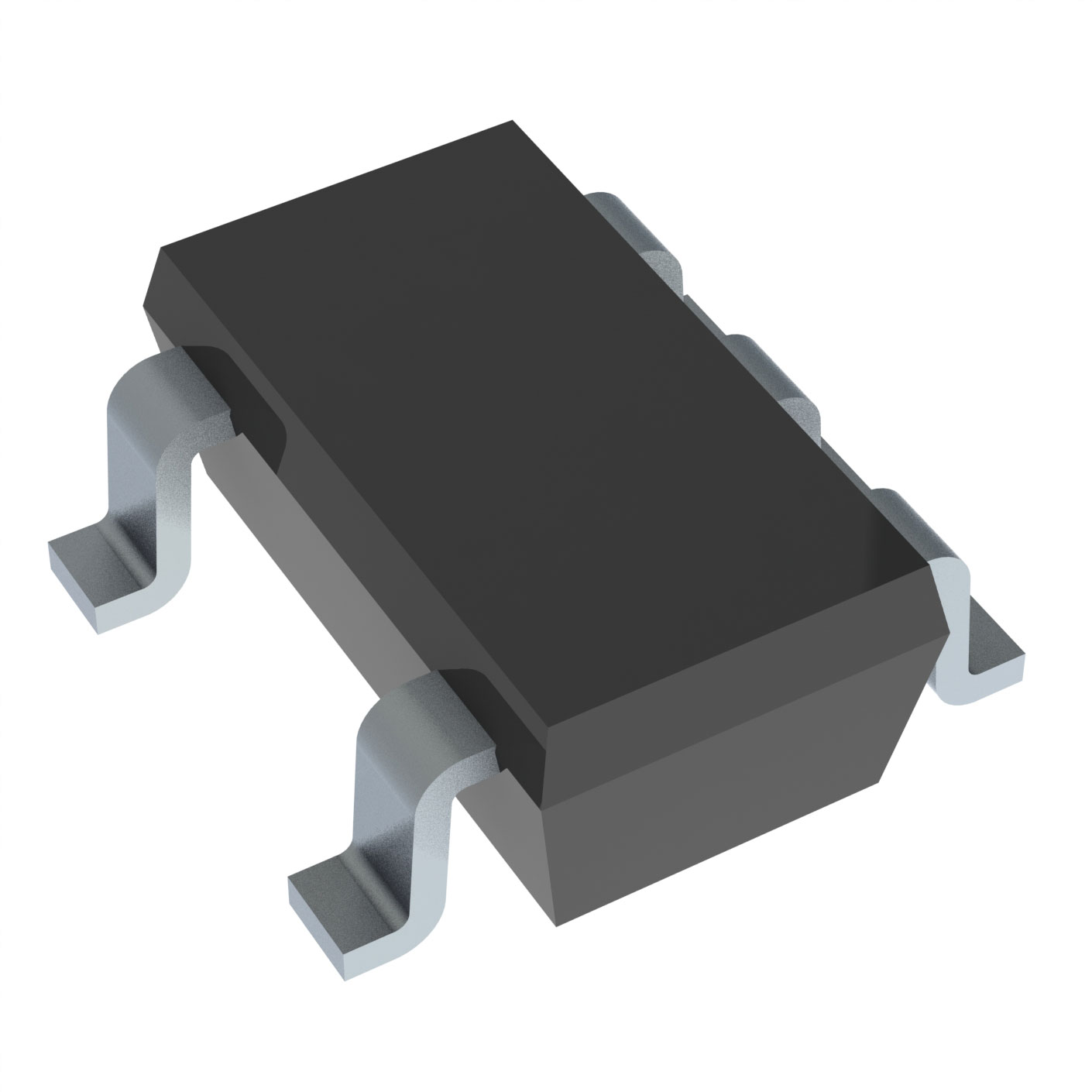
TLV2451CDBVR
OP Amps, Buffer Amps ICs


.png?x-oss-process=image/format,webp/resize,p_30)


TLV2451CDBVR Description
TLV2451CDBVR Description
The TLV2451CDBVR is a high-performance operational amplifier (op-amp) from Texas Instruments, designed for general-purpose applications. It offers a unique combination of features that make it an ideal choice for various electronic systems. With a supply voltage range of 2.7V to 6V, it can operate efficiently in a wide range of power supply conditions. The device is RoHS3 compliant, making it suitable for environmentally friendly applications.
TLV2451CDBVR Features
- Voltage - Supply Span (Max): 6V
- Voltage - Supply Span (Min): 2.7V
- Gain Bandwidth Product: 220 kHz
- Slew Rate: 0.11V/µs
- Current - Input Bias: 500 pA
- Current - Supply: 23µA
- Current - Output / Channel: 10 mA
- Voltage - Input Offset: 300 µV
- Operating Temperature: 0°C ~ 70°C
- Mounting Type: Surface Mount
- Package: Tape & Reel (TR)
- Number of Circuits: 1
- Amplifier Type: General Purpose
- REACH Status: REACH Unaffected
- Moisture Sensitivity Level (MSL): 1 (Unlimited)
- ECCN: EAR99
- HTSUS: 8542.33.0001
TLV2451CDBVR Applications
The TLV2451CDBVR is ideal for a variety of applications due to its robust performance and versatile features. Some specific use cases include:
- Audio Amplification: Its high slew rate and low input bias current make it suitable for audio circuits where fast response and low noise are critical.
- Sensor Signal Conditioning: The device's low offset voltage and low noise characteristics are ideal for conditioning signals from sensors in industrial and consumer applications.
- Data Acquisition Systems: Its high gain bandwidth product and low power consumption make it suitable for data acquisition systems in IoT devices and other electronic systems.
- Automotive Applications: The device's wide operating temperature range and low power consumption make it suitable for use in automotive electronics, such as sensor interfaces and control systems.
Conclusion of TLV2451CDBVR
The TLV2451CDBVR is a versatile and high-performance op-amp from Texas Instruments, offering a unique combination of features that make it suitable for a wide range of applications. Its low power consumption, high gain bandwidth product, and low input bias current make it an ideal choice for audio amplification, sensor signal conditioning, data acquisition systems, and automotive applications. With its RoHS3 compliance and REACH unaffected status, the TLV2451CDBVR is also an environmentally friendly option for electronic system designers.
Tech Specifications
TLV2451CDBVR Documents
Download datasheets and manufacturer documentation for TLV2451CDBVR
 Assembly/Wafer Fab Site 31/Jul/2023
  TLV2450-55, TLV245xA
 Shopping Guide


.png?x-oss-process=image/format,webp/resize,h_32)


