
Texas Instruments
TLV2452CDR
OP Amps, Buffer Amps ICs


.png?x-oss-process=image/format,webp/resize,p_30)


TLV2452CDR Description
TLV2452CDR Description
The TLV2452CDR is a high-performance, general-purpose operational amplifier (op-amp) from Texas Instruments, designed for a wide range of applications. This dual-channel op-amp features a supply voltage range from 2.7V to 6V, making it suitable for both low-voltage and standard voltage applications. With a gain bandwidth product of 220 kHz and a slew rate of 0.11V/µs, the TLV2452CDR offers excellent performance in signal processing and amplification tasks.
TLV2452CDR Features
- Wide Supply Voltage Range: The TLV2452CDR operates within a supply voltage range of 2.7V to 6V, providing flexibility for various power supply configurations.
- Low Input Bias Current: With an input bias current of only 500 pA, the TLV2452CDR minimizes the impact of input currents on the signal, ensuring high accuracy and stability.
- Low Supply Current: The device consumes only 23µA per channel, making it highly energy-efficient and suitable for battery-powered and low-power applications.
- Low Input Offset Voltage: The input offset voltage of 300 µV ensures minimal error in signal processing, enhancing the accuracy of the amplifier.
- High Output Current: Each channel can drive up to 10 mA, allowing the TLV2452CDR to drive moderate loads directly.
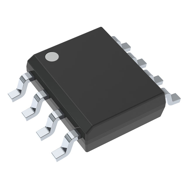
- Surface Mount Packaging: The TLV2452CDR is available in an 8-SOIC package, which is ideal for surface mount applications, providing a compact and reliable solution for PCB designs.
- Compliance and Reliability: The TLV2452CDR is REACH unaffected and RoHS3 compliant, ensuring environmental sustainability and regulatory compliance. It also has a moisture sensitivity level (MSL) of 1, making it suitable for unlimited storage conditions.
TLV2452CDR Applications
The TLV2452CDR is ideal for a variety of applications due to its versatile performance characteristics:
- Signal Conditioning: The low input offset voltage and low input bias current make the TLV2452CDR suitable for precision signal conditioning in sensor interfaces and instrumentation.
- Audio Applications: The dual-channel design and moderate bandwidth make it suitable for audio amplification and processing tasks, ensuring high fidelity and low distortion.
- Battery-Powered Devices: The low supply current and wide supply voltage range make the TLV2452CDR ideal for portable and battery-powered applications, where power efficiency is critical.
- General-Purpose Amplification: The TLV2452CDR's general-purpose design makes it suitable for a wide range of amplification tasks, from simple gain stages to more complex signal processing circuits.
Conclusion of TLV2452CDR
The TLV2452CDR from Texas Instruments is a versatile and high-performance operational amplifier that offers a balance of low power consumption, wide supply voltage range, and high accuracy. Its low input bias current and low input offset voltage ensure minimal signal distortion, making it ideal for precision applications. The dual-channel design and moderate bandwidth make it suitable for a wide range of applications, from audio processing to general-purpose amplification. The TLV2452CDR's compliance with environmental and regulatory standards, along with its surface mount packaging, ensures reliability and ease of integration into modern electronic designs.
Tech Specifications
TLV2452CDR Documents
Download datasheets and manufacturer documentation for TLV2452CDR
 Mechanical Outline Drawing
  Product Change Notification 2024-02-08 (PDF) Product Change Notification (PDF)
  TLV2452CDR Symbol & Footprint by SnapMagic
  TLV245xA PSpice 5V Supply Voltage Model
 Shopping Guide


.png?x-oss-process=image/format,webp/resize,h_32)


