
Texas Instruments
TLV2452ID
OP Amps, Buffer Amps ICs


.png?x-oss-process=image/format,webp/resize,p_30)


TLV2452ID Description
TLV2452ID Description
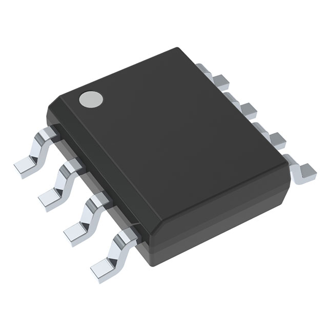
The TLV2452ID from Texas Instruments is a general-purpose operational amplifier (op-amp) featuring dual-channel functionality in an 8-SOIC package. Designed for low-power applications, it operates over a 2.7V to 6V supply range, making it ideal for battery-powered and portable electronics. With an ultra-low input bias current of 500 pA and a moderate gain bandwidth product (GBWP) of 220 kHz, it balances precision and efficiency. The device exhibits a low input offset voltage (300 µV) and a slew rate of 0.11V/µs, ensuring stable performance in signal conditioning and amplification tasks. Its RoHS3 compliance and REACH-unaffected status make it environmentally friendly for modern designs.
TLV2452ID Features
- Low Power Consumption: 23µA per channel supply current extends battery life in portable devices.
- Wide Supply Range: 2.7V–6V operation supports diverse power sources.
- High Input Impedance: 500 pA input bias current minimizes loading effects in high-impedance circuits.
- Moderate Speed: 220 kHz GBWP and 0.11V/µs slew rate suit low-frequency signal processing.
- Robust Output: 10 mA output current drives modest loads without external buffering.
- Reliable Packaging: 8-SOIC tube packaging ensures mechanical and thermal stability.
- Environmental Compliance: ROHS3 and REACH-unaffected for global regulatory adherence.
TLV2452ID Applications
- Sensor Interfaces: Ideal for amplifying signals from thermocouples, strain gauges, and photodiodes due to low input bias current.
- Battery-Powered Systems: Energy-efficient operation suits wearables, IoT nodes, and medical devices.
- Signal Conditioning: Filters, integrators, and buffers benefit from its low offset and noise performance.
- Industrial Control: Wide supply range accommodates PLC analog front-ends and instrumentation.
- Consumer Electronics: Used in audio preamps, volume controls, and low-power signal chains.
Conclusion of TLV2452ID
The TLV2452ID stands out as a versatile, low-power op-amp for precision analog designs. Its ultra-low input bias, wide voltage range, and dual-channel integration make it superior to basic op-amps like the LM358, particularly in high-impedance or battery-critical applications. Engineers can leverage its balanced performance and compliance for portable, industrial, and sensor-based systems where reliability and efficiency are paramount.
Tech Specifications
TLV2452ID Documents
Download datasheets and manufacturer documentation for TLV2452ID
 Assembly/Wafer Fab Site 31/Jul/2023
  TLV2450-55, TLV245xA
 Shopping Guide


.png?x-oss-process=image/format,webp/resize,h_32)


